


Memory Protection Unit in Embedded Systems

Table Of Contents
Introduction
In safety-critical and security-sensitive embedded systems, a stray pointer or a buffer overflow in one task can corrupt the memory of another — leading to catastrophic failures that are incredibly difficult to debug. The Memory Protection Unit (MPU) is a hardware feature available on most ARM Cortex-M processors that provides a first line of defense against such memory access violations. By dividing the memory map into regions with individually configurable access permissions, the MPU can detect and trap illegal memory accesses before they cause irreparable damage.
This article explores how the MPU works, how to configure it, and how it integrates with real-time operating systems to create robust, fault-resilient firmware.
What Is the MPU?
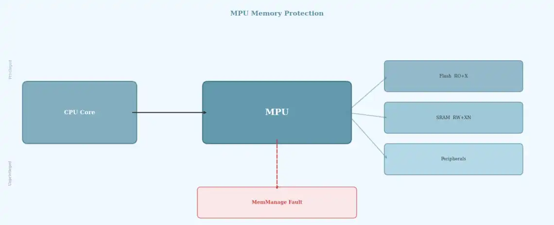
The MPU is an optional hardware unit integrated into ARM Cortex-M3, M4, M7, and some Cortex-M23/M33 processors. Cortex-M0/M0+ cores do not include a standard ARM MPU, though some vendors provide similar proprietary protection mechanisms. It monitors every memory access made by the CPU and compares it against a set of programmer-defined rules. If an access violates the configured permissions, the processor raises a Memory Management Fault (MemManage) exception, allowing the firmware to log the error, recover, or take corrective action.
Unlike a full Memory Management Unit (MMU) found in application processors, the MPU does not perform address translation or support virtual memory. It operates on the physical address map, making it lightweight and deterministic — ideal for real-time embedded applications.
MPU Architecture and Registers
The ARMv7-M MPU (found on Cortex-M3/M4/M7) supports up to eight independently configurable memory regions, each of which can be subdivided into eight subregions. The Cortex-M7 extends this to 16 regions, but this is implementation-dependent. Each region is configured using the following registers:
- MPU_RNR (Region Number Register): Selects which region (0–7 or 0–15) to configure.
- MPU_RBAR (Region Base Address Register): Specifies the base address of the region.
- MPU_RASR (Region Attribute and Size Register): Defines the region size, access permissions, memory type, and enable flag.
The MPU_CTRL (Control Register) enables the MPU and optionally activates the background region, which applies the default memory map to privileged accesses for addresses not covered by any MPU region.
Access Permission (AP) Field
The AP field in RASR controls read/write access for both privileged and unprivileged modes:
| AP Value | Privileged Mode | User Mode |
|---|---|---|
| 000 | No Access | No Access |
| 001 | Read/Write | No Access |
| 010 | Read/Write | Read Only |
| 011 | Read/Write | Read/Write |
| 100 | (Reserved) | (Reserved) |
| 101 | Read Only | No Access |
| 110 | Read Only | Read Only |
| 111 | Read Only | Read Only |
*Note: Some AP encodings (e.g., 111) may be implementation-defined but typically behave as read-only for both modes.
Execute Never (XN) Bit
Setting the XN bit on a region prevents the processor from executing code from that memory area. This is critical for security: it prevents an attacker (or a bug) from executing data as code, thwarting code injection attacks.
Configuring the MPU: Step by Step
A typical MPU configuration follows this sequence:
/* Step 1: Enable the MemManage fault exception */SCB->SHCSR |= SCB_SHCSR_MEMFAULTENA_Msk;/* Step 2: Configure Region 0 — Flash (Read-Only, Executable) */MPU->RNR = 0;MPU->RBAR = 0x08000000 | MPU_RBAR_VALID_Msk | 0;MPU->RASR = MPU_RASR_ENABLE_Msk| (0x13 << MPU_RASR_SIZE_Pos) /* 1MB region (Size = 19, 2^(19+1) = 1MB) */| (0x06 << MPU_RASR_AP_Pos) /* P:RO, U:RO */| (0x01 << MPU_RASR_TEX_Pos); /* Normal, cacheable *//* Step 3: Configure Region 1 — SRAM (Read/Write, No Execute) */MPU->RNR = 1;MPU->RBAR = 0x20000000 | MPU_RBAR_VALID_Msk | 1;MPU->RASR = MPU_RASR_ENABLE_Msk| (0x11 << MPU_RASR_SIZE_Pos) /* 256KB region (Size = 17, 2^(17+1) = 256KB) */| (0x03 << MPU_RASR_AP_Pos) /* P:RW, U:RW */| MPU_RASR_XN_Msk /* Execute Never */| (0x01 << MPU_RASR_TEX_Pos);/* Step 4: Configure Region 2 — Peripherals (Privileged Only) */MPU->RNR = 2;MPU->RBAR = 0x40000000 | MPU_RBAR_VALID_Msk | 2;MPU->RASR = MPU_RASR_ENABLE_Msk| (0x1C << MPU_RASR_SIZE_Pos) /* 512MB region (Size = 28, 2^(28+1) = 512MB) */| (0x01 << MPU_RASR_AP_Pos) /* P:RW, U:No Access */| MPU_RASR_XN_Msk| (0x02 << MPU_RASR_TEX_Pos); /* Device memory (via TEX/C/B configuration) *//* Step 5: Enable MPU with default background map for privileged code */MPU->CTRL = MPU_CTRL_ENABLE_Msk | MPU_CTRL_PRIVDEFENA_Msk;
Note: Memory type is determined by a combination of TEX, C, B, and S bits, not by TEX alone.
Overlapping Regions and Subregions
When two MPU regions overlap, the region with the higher number takes precedence. This allows you to create a broad base region and overlay more specific restrictions on top. For example, Region 0 might grant read-only access to the entire flash, while Region 1 carves out a smaller subregion within flash that is read/write for a bootloader’s writable data section.
Each region of size 256 bytes or larger is automatically divided into eight subregions of equal size. The SRD (Subregion Disable) field in RASR lets you individually disable subregions, effectively creating non-contiguous protection areas without consuming additional region slots.
MPU in an RTOS Environment
The MPU truly shines when paired with an RTOS. In a typical RTOS configuration:
- Kernel code and data are placed in privileged-only regions, preventing user tasks from corrupting the kernel.
- Task stacks are placed in dedicated MPU regions with guard zones, enabling instant stack overflow detection.
- Peripherals can be assigned to specific tasks, preventing one task from accidentally reconfiguring another task’s hardware.
- Unprivileged tasks run in User mode and can only access their own memory regions.
FreeRTOS, for example, offers an MPU-aware port (FreeRTOS-MPU) that manages region configuration automatically during context switches. When the scheduler switches tasks, it loads the new task’s MPU region into the MPU registers, ensuring each task sees only its permitted memory regions.
Practical Benefits
- Bug Detection During Development: The MPU catches NULL pointer dereferences, buffer overflows, and stack overflows immediately — not hours later when corrupted data causes a mysterious failure.
- Security Hardening: By marking data regions as Execute Never and restricting peripheral access to privileged code only, the MPU significantly raises the bar for exploitation.
- Safety Compliance: Standards like IEC 61508 (functional safety) and DO-178C (avionics) require memory protection. The MPU provides a hardware mechanism to satisfy these requirements on Cortex-M processors.
- Task Isolation: In systems running third-party code or untrusted modules, the MPU sandboxes each module, preventing it from accessing memory belonging to other components.
Common Pitfalls
- Forgetting to enable MemManage fault: Without
SCB_SHCSR_MEMFAULTENA_Msk, an MPU violation triggers a HardFault instead of a MemManage fault, making debugging harder. - Region size must be a power of two: The MPU requires region sizes to be powers of two (from 32 bytes to 4 GB), and the base address must be aligned to the region size.
- Not using PRIVDEFENA: Without the background region enabled, any address not covered by an explicit region will fault — even for privileged code. Enable
PRIVDEFENAunless you explicitly cover the entire address space. - Interrupt latency: The MPU does not significantly impact memory access timing in most implementations, but the system-level effects (such as faults and context switching) must be considered in real-time analysis.
Summary
The Memory Protection Unit is one of the most underutilized features in embedded Cortex-M development. With just a handful of register writes, you can transform a fragile firmware into a resilient system that detects and contains memory access violations in real time. Whether you are building a safety-critical medical device, an automotive ECU, or an IoT product that needs to resist tampering, the MPU provides hardware-enforced memory protection with minimal performance overhead. Integrating it with your RTOS task model is the key to achieving true task isolation and system robustness.
Frequently Asked Questions
What is the role of a Memory Protection Unit (MPU)?
An MPU divides the microcontroller's memory map into regions and enforces access rules (read/write/execute). It detects memory corruption, stack overflows, and unauthorized access, triggering a hard fault exception.
How does an MPU improve RTOS security?
The MPU allows running tasks in non-privileged (user) mode, preventing them from accessing hardware registers directly or writing into the memory space of other tasks, isolating faults.
What are the limitations of an MPU compared to an MMU?
An MPU only defines access permissions for physical memory blocks (typically limited to 8-16 regions). An MMU (Memory Management Unit) supports virtual memory and address translation, which is required for operating systems like Linux.
Related Posts

Rate Monotonic Scheduling and Schedulability Analysis in RTOS
June 22, 2026
5 min

RTOS Performance Profiling and Optimization Techniques
June 10, 2026
3 min
Quick Links
Legal Stuff