

Fixing I2C Clock Stretching Timeouts on STM32
July 07, 2026
3 min
When your STM32 acts as an SPI slave in a high-speed data acquisition chain — streaming ADC samples, forwarding sensor frames, or bridging to a host processor — the bottleneck is rarely the SPI clock rate. It’s the firmware’s ability to keep pace with incoming bytes. At 25 MHz SPI, a byte arrives every 320 ns. An interrupt-driven RXNE read takes 500-800 ns just to enter the ISR. The math doesn’t work.
DMA changes the equation: the peripheral moves data directly to RAM while the CPU executes application logic. This article details a production-ready SPI slave DMA implementation on STM32, covering hardware NSS handling, circular buffer management, frame boundary detection, and the timing constraints that determine whether your acquisition chain keeps up or drops frames.
SPI master implementations are well documented. The slave side — where your MCU receives data from an external controller (FPGA, another MCU, DSP) — is less common but critical for:
In all cases, the external master controls the clock. Your firmware must consume bytes at line rate without backpressure.
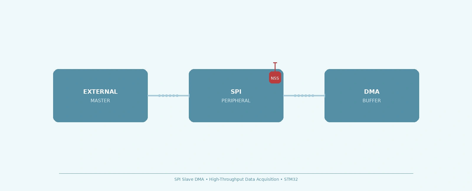
+-------------------+ +-------------------+ +-------------------+| | SCLK | | RX | || |------->| STM32 SPI |=======>| DMA Stream 0 || External Master | MOSI | Peripheral | Data | (Memory Buffer) || (FPGA, MCU, DSP) |------->| (Slave Mode) | | || | | | | || | NSS | | | || |---+--->| Hardware NSS | +-------------------++-------------------+ | +-------------------+ || | HT/TC/TE| | Interrupts| +-------------------+ v| | | +-------------------+'--->| EXTI / GPIO | ISR | || (Frame Detect) |------->| Application || | Flag | Processing |+-------------------+ +-------------------+
Key STM32 SPI slave registers for DMA:
| Register | Field | Purpose |
|---|---|---|
CR1 | SPE, MSTR=0 | Enable SPI, configure as slave |
CR2 | RXDMAEN, SSOE=0 | Enable RX DMA, hardware NSS management |
SR | RXNE, OVR, FRE | Status flags for polling/debug |
DR | Data register | DMA source address (peripheral) |
The NSS (Chip Select) pin is the only hardware signal that delimits SPI frames in slave mode. Unlike master mode where software toggles NSS, slave mode requires the external master to drive NSS. STM32 supports two NSS modes:
Hardware NSS (SSM=0, SSOE=0 in CR1/CR2):
RXNE may still be set for last byteSoftware NSS (SSM=1):
SSI bit in CR1 acts as internal NSSAlways use hardware NSS. Connect the master’s CS to the STM32 NSS pin (PA4, PB12, etc. depending on SPI instance and AF mapping).
The core challenge: DMA doesn’t know about SPI frames. It fills a linear or circular buffer continuously. You must correlate NSS edges with DMA position to extract valid frames.
/* STM32F4 SPI1 Slave DMA Configuration */#define SPI_SLAVE_DMA_BUFFER_SIZE 4096 /* Must be power of 2 for fast modulo */#define SPI_SLAVE_MAX_FRAME_SIZE 2048 /* Largest expected frame from master */static uint8_t spi_rx_buffer[SPI_SLAVE_DMA_BUFFER_SIZE] __attribute__((aligned(32)));static volatile uint16_t frame_start_idx = 0;static volatile uint16_t frame_end_idx = 0;static volatile bool frame_ready = false;/* DMA2 Stream 0 (SPI1_RX) or Stream 2 (SPI1_RX on some variants) */void spi_slave_dma_init(void){/* 1. Enable clocks */RCC->AHB1ENR |= RCC_AHB1ENR_DMA2EN;RCC->APB2ENR |= RCC_APB2ENR_SPI1EN;RCC->AHB1ENR |= RCC_AHB1ENR_GPIOAEN;RCC->APB2ENR |= RCC_APB2ENR_SYSCFGEN; /* Required for EXTI configuration *//* 2. GPIO: PA5=SCK, PA6=MISO, PA7=MOSI, PA4=NSS (AF5 for SPI1) */GPIOA->MODER &= ~(GPIO_MODER_MODE4 | GPIO_MODER_MODE5 | GPIO_MODER_MODE6 | GPIO_MODER_MODE7);GPIOA->MODER |= (GPIO_MODER_MODE4_1 | GPIO_MODER_MODE5_1 | GPIO_MODER_MODE6_1 | GPIO_MODER_MODE7_1);GPIOA->AFR[0] &= ~(GPIO_AFRL_AFSEL4 | GPIO_AFRL_AFSEL5 | GPIO_AFRL_AFSEL6 | GPIO_AFRL_AFSEL7);GPIOA->AFR[0] |= (5 << GPIO_AFRL_AFSEL4_Pos) | (5 << GPIO_AFRL_AFSEL5_Pos) |(5 << GPIO_AFRL_AFSEL6_Pos) | (5 << GPIO_AFRL_AFSEL7_Pos);GPIOA->OSPEEDR |= (3 << GPIO_OSPEEDR_OSPEED4_Pos) | (3 << GPIO_OSPEEDR_OSPEED5_Pos) |(3 << GPIO_OSPEEDR_OSPEED6_Pos) | (3 << GPIO_OSPEEDR_OSPEED7_Pos);/* 3. NSS rising/falling edge interrupt (EXTI4) */SYSCFG->EXTICR[1] &= ~SYSCFG_EXTICR2_EXTI4;SYSCFG->EXTICR[1] |= SYSCFG_EXTICR2_EXTI4_PA;EXTI->IMR |= EXTI_IMR_MR4;EXTI->RTSR |= EXTI_RTSR_TR4; /* Rising edge = frame end */EXTI->FTSR |= EXTI_FTSR_TR4; /* Falling edge = frame start */NVIC_SetPriority(EXTI4_IRQn, 5);NVIC_EnableIRQ(EXTI4_IRQn);/* 4. SPI1 Slave Configuration */SPI1->CR1 = 0; /* SPI must be disabled for config */SPI1->CR1 &= ~SPI_CR1_MSTR; /* Slave mode */SPI1->CR1 &= ~SPI_CR1_SSM; /* Hardware NSS */SPI1->CR1 &= ~SPI_CR1_SSI;SPI1->CR1 &= ~SPI_CR1_DFF; /* 8-bit data frame (robust for variable length) */SPI1->CR1 &= ~(SPI_CR1_CPOL | SPI_CR1_CPHA); /* Mode 0: adjust per master *//* 5. SPI1 CR2: RX DMA enable, hardware NSS */SPI1->CR2 = 0;SPI1->CR2 |= SPI_CR2_RXDMAEN; /* Enable RX DMA */SPI1->CR2 &= ~SPI_CR2_SSOE; /* NSS input (slave) *//* 6. DMA2 Stream 0 (SPI1_RX) - Circular mode */DMA2_Stream0->CR = 0;DMA2_Stream0->PAR = (uint32_t)&SPI1->DR; /* Peripheral: SPI data register */DMA2_Stream0->M0AR = (uint32_t)spi_rx_buffer; /* Memory: circular buffer */DMA2_Stream0->NDTR = SPI_SLAVE_DMA_BUFFER_SIZE; /* Count in bytes */DMA2_Stream0->CR |= (3 << DMA_SxCR_CHSEL_Pos); /* Channel 3 for SPI1_RX */DMA2_Stream0->CR |= DMA_SxCR_PL_1; /* High priority */DMA2_Stream0->CR &= ~DMA_SxCR_MSIZE; /* 8-bit peripheral size */DMA2_Stream0->CR &= ~DMA_SxCR_PSIZE; /* 8-bit memory size */DMA2_Stream0->CR |= DMA_SxCR_MINC; /* Memory increment */DMA2_Stream0->CR |= DMA_SxCR_CIRC; /* Circular mode */DMA2_Stream0->CR |= DMA_SxCR_TCIE | DMA_SxCR_HTIE; /* Transfer complete + half-transfer IRQs */DMA2_Stream0->CR |= DMA_SxCR_TEIE | DMA_SxCR_DMEIE; /* Error interrupts *//* 7. Enable DMA stream */DMA2_Stream0->CR |= DMA_SxCR_EN;/* 8. DMA interrupt */NVIC_SetPriority(DMA2_Stream0_IRQn, 6);NVIC_EnableIRQ(DMA2_Stream0_IRQn);/* 9. Enable SPI */SPI1->CR1 |= SPI_CR1_SPE;}
The EXTI interrupt on NSS pin captures frame start/end with near-zero latency:
void EXTI4_IRQHandler(void){if (EXTI->PR & EXTI_PR_PR4) {EXTI->PR = EXTI_PR_PR4; /* Clear pending */bool nss_state = (GPIOA->IDR & (1 << 4)) != 0; /* Read NSS pin (PA4) */if (!nss_state) {/* NSS FALLING: Frame start */frame_start_idx = SPI_SLAVE_DMA_BUFFER_SIZE - DMA2_Stream0->NDTR;frame_ready = false;} else {/* NSS RISING: Frame end */frame_end_idx = SPI_SLAVE_DMA_BUFFER_SIZE - DMA2_Stream0->NDTR;frame_ready = true;}}}
Critical timing note: The NSS rising edge interrupt fires after the last SCLK edge but before the DMA writes the final byte to memory (DMA runs on AHB bus, SPI on APB). The frame_end_idx may point one position past the last valid byte. Handle this in processing:
void process_spi_frame(void){if (!frame_ready) return;uint16_t start = frame_start_idx;uint16_t end = frame_end_idx;uint16_t len = (end >= start) ? (end - start) : (SPI_SLAVE_DMA_BUFFER_SIZE - start + end);/* Clamp to max frame size (sanity check) */if (len > SPI_SLAVE_MAX_FRAME_SIZE) len = SPI_SLAVE_MAX_FRAME_SIZE;/* Frame data wraps at buffer boundary? */if (start + len <= SPI_SLAVE_DMA_BUFFER_SIZE) {/* Contiguous */handle_frame_data(&spi_rx_buffer[start], len);} else {/* Wrapped: copy to linear buffer for processing */static uint8_t linear_buf[SPI_SLAVE_MAX_FRAME_SIZE];uint16_t first_chunk = SPI_SLAVE_DMA_BUFFER_SIZE - start;memcpy(linear_buf, &spi_rx_buffer[start], first_chunk);memcpy(&linear_buf[first_chunk], spi_rx_buffer, len - first_chunk);handle_frame_data(linear_buf, len);}frame_ready = false;}
For very long frames (larger than buffer), or to process streaming data before frame end, use DMA HT/TC interrupts:
void DMA2_Stream0_IRQHandler(void){uint32_t isr = DMA2->LISR;DMA2->LIFCR = DMA_LIFCR_CTCIF0 | DMA_LIFCR_CHTIF0 | DMA_LIFCR_CTEIF0;if (isr & DMA_LISR_HTIF0) {/* Half-transfer: first half of buffer filled *//* Process data from frame_start_idx to buffer midpoint */uint16_t half_idx = SPI_SLAVE_DMA_BUFFER_SIZE / 2; /* In bytes *//* ... process chunk ... */}if (isr & DMA_LISR_TCIF0) {/* Transfer-complete: buffer wrapped *//* Process data from midpoint to end *//* ... process chunk ... */}if (isr & DMA_LISR_TEIF0) {/* Transfer error: bus fault, stop DMA */DMA2_Stream0->CR &= ~DMA_SxCR_EN;/* Log error, trigger recovery */}}
| Technique | Impact | Implementation |
|---|---|---|
| 16-bit/32-bit DMA | 2-4x fewer bus cycles | DFF=1 in SPI CR1, MSIZE=PSIZE=16/32-bit in DMA |
| High DMA priority | Reduces bus contention | PL=10 (high) in DMA CR |
| DTCM/TCM RAM for buffer | Zero wait states | Place buffer in DTCMRAM or SRAM2 (H7) |
| Disable flash ART/prefetch for DMA | Prevents bus conflicts | Not always needed; profile first |
| Minimize ISR overhead | Frees CPU cycles | No printf, no locks, flag-based signaling only |
| Align buffer to cache line | Prevents cache thrashing | 32-byte alignment for Cortex-M7 |
| Symptom | Root Cause | Fix |
|---|---|---|
| First byte of frame lost | EXTI ISR delayed; reads NDTR after 1st byte DMA’d, corrupting start index | Master must add delay between NSS falling edge and first SCLK edge |
| Last byte corrupted | NSS rising before DMA writes final byte | Master must hold NSS low for 1 extra SCLK cycle after last bit |
| OVR flag set, data lost | DMA buffer too small / CPU stalled too long | Increase buffer, enable HT/TC interrupts for early processing |
| Frame length varies unexpectedly | Master sends variable lengths; NDTR snapshot at wrong time | Use circular DMA + NSS ISR to measure actual bytes per frame |
| DMA stops after 1 frame | Circular mode not set / NDTR not reloaded | Verify CIRC bit, NDTR auto-reloads in circular mode |
# 1. Verify SPI clock polarity/phase matches master# Scope SCLK/MOSI at STM32 pins — check first edge timing# 2. Verify NSS timing# NSS must go low >= 1 SCLK period before first clock edge# NSS must stay low >= 1 SCLK period after last clock edge# 3. Measure throughput# Send known frame size, timestamp NSS edges via GPIO toggle# Calculate: bytes / (NSS_rising - NSS_falling)# 4. Stress test# Continuous max-size frames at max SPI clock# Monitor OVR flag, DMA error flags, buffer overrun# 5. Validate data integrity# Master sends incrementing pattern or CRC# STM32 verifies every frame
SPI slave DMA on STM32 transforms the MCU from a byte-at-a-time interrupt handler into a high-throughput data mover. The architecture is straightforward: hardware NSS captures frame boundaries via EXTI, circular DMA absorbs the byte stream, and application code correlates NSS edges with DMA position to extract valid frames.
Key takeaways:
For production systems, wrap this in a double-buffered ping-pong scheme where the DMA fills buffer A while the CPU processes buffer B, swapping on NSS rising edge. That eliminates the copy-on-wrap and achieves true zero-copy throughput.
Quick Links
Legal Stuff