

UART Overrun Errors in STM32: Fixing with DMA
September 18, 2026
4 min
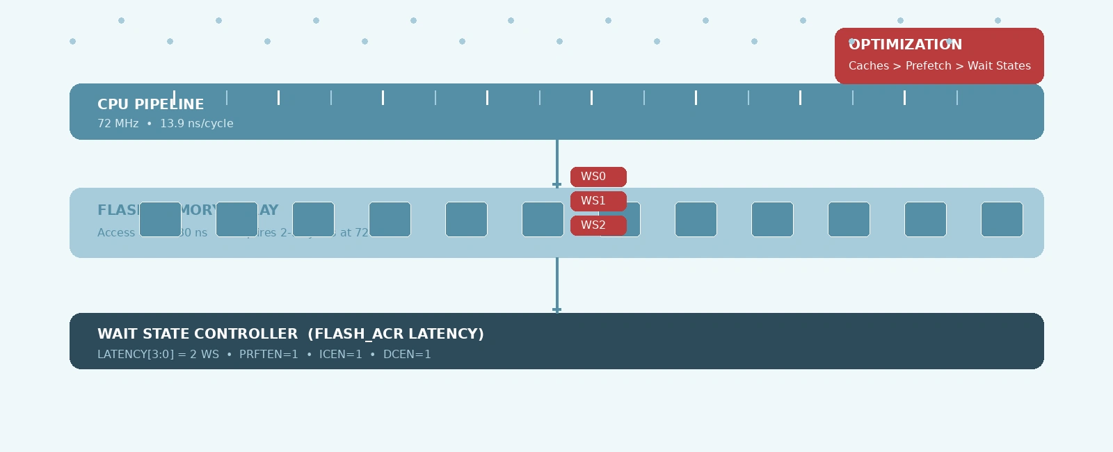
Flash wait states (access latency) represent one of the most critical hardware configuration parameters on ARM Cortex-M microcontrollers. While modern Cortex-M cores (Cortex-M3, M4, M7, M33, M55, M85) easily clock between 72 MHz and 1 GHz, embedded NOR flash memory physics impose fundamental access delays of 20 ns to 40 ns.
If the core clock period is shorter than the flash access time, the memory controller must insert wait states—holding the CPU pipeline while the flash array charges wordlines and sense amplifiers evaluate bit cells.
In safety-critical applications governed by standards like ISO 26262 (ASIL D), IEC 61508 (SIL 3/4), DO-254/DO-178C (DAL A), and IEC 62304, flash timing configuration is not just a performance knob; it directly impacts Worst-Case Execution Time (WCET), instruction bus integrity, and hardware fault injection resilience (ECC/parity errors).
+-------------------------------------------------------------------------------+| ARM Cortex-M Core Engine || || +--------------------+ ICode / DCode Bus +--------------------------+ || | Execution Pipeline | <=====================> | Flash Memory Controller | || +--------------------+ +--------------------------+ || | | || | Core Clock (168 MHz = 5.95 ns) | Access Delay || v v || 1 CPU Cycle = 5.95 ns Flash Array = ~35.7 ns || (Requires 5 Wait States) |+-------------------------------------------------------------------------------+
Embedded non-volatile flash (eFlash) consists of floating-gate or charge-trap transistors. Reading a flash cell requires pre-charging bitlines, driving wordlines to a reference voltage, and allowing differential sense amplifiers to discriminate between programmed (charged) and erased states.
This analog sensing process has a fixed physical delay: $T_{acc} \approx 20\text{ ns to }35\text{ ns}$.
Total Flash Access Time = (LATENCY + 1) * T_CPU_CLK
Where:
Assuming a typical flash access delay of $T_{acc} = 30\text{ ns}$:
| SYSCLK (HCLK) | Clock Period ($T_{cyc}$) | Min CPU Cycles Required | Required Wait States ($N$) | Total Read Latency |
|---|---|---|---|---|
| 16 MHz | 62.50 ns | 1 cycle ($62.5\text{ ns} \ge 30\text{ ns}$) | 0 WS | 62.50 ns |
| 30 MHz | 33.33 ns | 1 cycle ($33.33\text{ ns} \ge 30\text{ ns}$) | 0 WS | 33.33 ns |
| 60 MHz | 16.67 ns | 2 cycles ($33.33\text{ ns} \ge 30\text{ ns}$) | 1 WS | 33.33 ns |
| 90 MHz | 11.11 ns | 3 cycles ($33.33\text{ ns} \ge 30\text{ ns}$) | 2 WS | 33.33 ns |
| 120 MHz | 8.33 ns | 4 cycles ($33.33\text{ ns} \ge 30\text{ ns}$) | 3 WS | 33.33 ns |
| 150 MHz | 6.67 ns | 5 cycles ($33.33\text{ ns} \ge 30\text{ ns}$) | 4 WS | 33.33 ns |
| 168 MHz | 5.95 ns | 6 cycles ($35.71\text{ ns} \ge 30\text{ ns}$) | 5 WS | 35.71 ns |
If the CPU clock runs at 168 MHz (5.95 ns per cycle) and software configures 0 wait states, the core will sample the ICode data bus at 5.95 ns—long before the flash sense amplifiers settle. The result is bus noise, decoding garbage opcodes, executing invalid instructions (Undefined Instruction UndefFault), or triggering a BusFault / HardFault.
A common misconception among firmware developers is that lower operating voltages allow fewer wait states. The exact opposite is true.
In CMOS logic and flash sense amplifiers, propagation delay $t_{pd}$ is inversely proportional to supply voltage:
$$t{pd} \propto \frac{C_L \cdot V{DD}}{(V{DD} - V{TH})^\alpha}$$
As $V_{DD}$ drops:
Wait States (LATENCY) | $V_{DD} = 2.7\text{V} - 3.6\text{V}$ | $V_{DD} = 2.4\text{V} - 2.7\text{V}$ | $V_{DD} = 2.1\text{V} - 2.4\text{V}$ | $V_{DD} = 1.8\text{V} - 2.1\text{V}$ |
|---|---|---|---|---|
| 0 WS (1 cycle) | $0 < \text{HCLK} \le 30\text{ MHz}$ | $0 < \text{HCLK} \le 24\text{ MHz}$ | $0 < \text{HCLK} \le 18\text{ MHz}$ | $0 < \text{HCLK} \le 16\text{ MHz}$ |
| 1 WS (2 cycles) | $30 < \text{HCLK} \le 60\text{ MHz}$ | $24 < \text{HCLK} \le 48\text{ MHz}$ | $18 < \text{HCLK} \le 36\text{ MHz}$ | $16 < \text{HCLK} \le 32\text{ MHz}$ |
| 2 WS (3 cycles) | $60 < \text{HCLK} \le 90\text{ MHz}$ | $48 < \text{HCLK} \le 72\text{ MHz}$ | $36 < \text{HCLK} \le 54\text{ MHz}$ | $32 < \text{HCLK} \le 48\text{ MHz}$ |
| 3 WS (4 cycles) | $90 < \text{HCLK} \le 120\text{ MHz}$ | $72 < \text{HCLK} \le 96\text{ MHz}$ | $54 < \text{HCLK} \le 72\text{ MHz}$ | $48 < \text{HCLK} \le 64\text{ MHz}$ |
| 4 WS (5 cycles) | $120 < \text{HCLK} \le 150\text{ MHz}$ | $96 < \text{HCLK} \le 120\text{ MHz}$ | $72 < \text{HCLK} \le 90\text{ MHz}$ | N/A |
| 5 WS (6 cycles) | $150 < \text{HCLK} \le 168\text{ MHz}$ | $120 < \text{HCLK} \le 144\text{ MHz}$ | $90 < \text{HCLK} \le 108\text{ MHz}$ | N/A |
| 6 WS (7 cycles) | N/A | $144 < \text{HCLK} \le 168\text{ MHz}$ | $108 < \text{HCLK} \le 120\text{ MHz}$ | N/A |
[!WARNING] Safety-Critical Mandate (ISO 26262 / IEC 61508 / DO-254): Never tune wait states based on typical bench measurements at $25^\circ\text{C}$ and nominal $3.3\text{V}$. You must select wait states based on the worst-case operational envelope:
- Minimum possible $V_{DD}$ prior to Brown-Out Reset (BOR) trip (e.g., $2.7\text{V}$ or $2.4\text{V}$).
- Maximum operating junction temperature $Tj = T_a + (P_D \times \theta{JA})$ up to $125^\circ\text{C}$.
- End-of-Life (EOL) flash cell degradation after maximum rated write/erase cycles. Violating datasheet timing margins invalidates FMEDA failure rate metrics ($\lambda$) and causes latent field failures under voltage sags or thermal extremes.
It is essential to distinguish between the standard ARM Cortex-M core architecture and vendor-specific flash controllers:
0x0000_0000 to 0x1FFF_FFFF) and DCode (literal pool constants and debug data)..rodata).SCB_EnableICache(), SCB_EnableDCache()).+-------------------------------------------------------------------------------+| STM32 ART Accelerator Architecture |+-------------------------------------------------------------------------------+| || ARM Core ICode Bus (32-bit Instructions) || | || +---> [ Instruction Cache: 64 lines x 128-bit ] ---> Hit: 0 WS (1 cyc)|| | || +---> [ Prefetch Buffer: 128-bit Queue ] ----------> Hit: 0 WS (1 cyc)|| | || +---> [ Embedded Flash Array (128-bit wide) ] -----> Miss: 5 WS (6 cyc)|| || ARM Core DCode Bus (32-bit Data / Constants) || | || +---> [ Data Cache: 8 lines x 128-bit ] -----------> Hit: 0 WS (1 cyc)|| |+-------------------------------------------------------------------------------+
When modifying system clock frequencies (such as during bootloader initialization, dynamic voltage/frequency scaling (DVFS), or entering/exiting low-power sleep modes), the order of operations is critical.
+-------------------------------------------------------------------------------+| Clock Frequency Scaling Sequencing Rules |+---------------------------------------+---------------------------------------+| SCENARIO A: Scaling Frequency UP | SCENARIO B: Scaling Frequency DOWN || (e.g., 16 MHz HSI -> 168 MHz PLL) | (e.g., 168 MHz PLL -> 16 MHz HSI) |+---------------------------------------+---------------------------------------+| | || 1. Configure NEW higher wait states | 1. Switch SYSCLK to lower clock || (e.g., FLASH_ACR = 5 WS) | (e.g., RCC_SYSCLKSource_HSI) || | | | || v | v || 2. Verify FLASH_ACR latency updated | 2. Verify clock switch complete || (Poll FLASH_ACR & LATENCY) | (Poll RCC_CFGR & SWS) || | | | || v | v || 3. Switch SYSCLK to high PLL clock | 3. Configure NEW lower wait states || (e.g., RCC_SYSCLKSource_PLL) | (e.g., FLASH_ACR = 0 WS) || | | | || v | v || 4. Verify clock switch complete | 4. Verify FLASH_ACR latency updated || (Poll RCC_CFGR & SWS) | (Poll FLASH_ACR & LATENCY) || | |+---------------------------------------+---------------------------------------+
[!CAUTION] Fatal Fault Condition: If you increase the PLL frequency to 168 MHz before configuring 5 wait states, the core will attempt to fetch the next instruction at 168 MHz with 0 wait states. The CPU will fetch corrupt opcodes within 1-2 clock cycles, entering a HardFault handler before the register write completes.
Below is an industrial-grade, safety-critical flash configuration module for STM32F4 microcontrollers implementing bounded timeout protection, cache invalidation sequences, and proper memory synchronization barriers.
/*** @file flash_latency_ctrl.c* @brief Safety-critical Flash Access Controller and Latency Configuration* @details Compliant with MISRA C:2012, featuring bounded timeouts and memory barriers.*/#include "stm32f4xx.h"#include <stdbool.h>#define FLASH_ACR_LATENCY_MASK (0x00000007U)#define FLASH_TIMEOUT_CYCLES (10000U)typedef enum {FLASH_STATUS_OK = 0x00U,FLASH_STATUS_ERROR_TIMEOUT = 0x01U,FLASH_STATUS_INVALID_PARAM = 0x02U} FlashStatus_t;/*** @brief Configures Flash latency, prefetch, and ART caches safely.* @param target_latency: Desired wait states (e.g., FLASH_ACR_LATENCY_5WS)* @param enable_prefetch: True to enable 128-bit prefetch queue* @param enable_icache: True to enable instruction cache* @param enable_dcache: True to enable data cache* @return FlashStatus_t: Result code*/FlashStatus_t Flash_Configure_Latency(uint32_t target_latency,bool enable_prefetch,bool enable_icache,bool enable_dcache){uint32_t timeout_counter = 0U;/* Validate parameter range (STM32F4 supports up to 7WS) */if ((target_latency & ~FLASH_ACR_LATENCY_MASK) != 0U) {return FLASH_STATUS_INVALID_PARAM;}/* 1. If disabling or resetting caches, clear enable bits first (RM0090 Section 3.5.1) */FLASH->ACR &= ~(FLASH_ACR_ICEN | FLASH_ACR_DCEN);/* 2. Reset instruction and data caches to prevent stale cache entries */FLASH->ACR |= (FLASH_ACR_ICRST | FLASH_ACR_DCRST);FLASH->ACR &= ~(FLASH_ACR_ICRST | FLASH_ACR_DCRST);/* 3. Prepare new ACR configuration value */uint32_t reg_val = FLASH->ACR;reg_val &= ~FLASH_ACR_LATENCY_MASK;reg_val |= target_latency;if (enable_prefetch) {reg_val |= FLASH_ACR_PRFTEN;} else {reg_val &= ~FLASH_ACR_PRFTEN;}if (enable_icache) {reg_val |= FLASH_ACR_ICEN;}if (enable_dcache) {reg_val |= FLASH_ACR_DCEN;}/* 4. Write back configuration to FLASH_ACR */FLASH->ACR = reg_val;/* 5. Data Synchronization Barrier to ensure register write commits */__DSB();__ISB();/* 6. Verify latency updated with bounded timeout (MISRA C:2012 Rule 14.4 / Dir 4.14) */while ((FLASH->ACR & FLASH_ACR_LATENCY_MASK) != target_latency) {timeout_counter++;if (timeout_counter >= FLASH_TIMEOUT_CYCLES) {return FLASH_STATUS_ERROR_TIMEOUT;}}return FLASH_STATUS_OK;}
To accurately measure the real performance penalty of flash wait states, developers use the ARM Cortex-M Data Watchpoint and Trace (DWT) Cycle Counter (DWT->CYCCNT).
However, standard naive cycle measurements often produce flawed results due to:
#include "stm32f4xx.h"/*** @brief Initialize DWT Cycle Counter on Cortex-M3/M4/M7*/void DWT_Init(void) {/* Enable TRCENA in CoreDebug DEMCR */CoreDebug->DEMCR |= CoreDebug_DEMCR_TRCENA_Msk;#if defined(DWT_LAR)/* Cortex-M7 / ARMv7E-M Software Lock Unlock */DWT->LAR = 0xC5ACCE55U;#endifDWT->CYCCNT = 0U;DWT->CTRL |= DWT_CTRL_CYCCNTENA_Msk;}/*** @brief Measures cycle execution time with full interrupt and barrier protection.*/uint32_t DWT_MeasureFunction(void (*target_func)(void)) {uint32_t start_cycles;uint32_t elapsed_cycles;/* Ensure all explicit memory transactions complete */__DSB();__ISB();/* Disable interrupts to ensure measurement determinism */uint32_t primask = __get_PRIMASK();__disable_irq();/* Memory clobber barrier prevents compiler reordering */__asm volatile("" ::: "memory");start_cycles = DWT->CYCCNT;__asm volatile("" ::: "memory");target_func();__asm volatile("" ::: "memory");elapsed_cycles = DWT->CYCCNT - start_cycles;__asm volatile("" ::: "memory");/* Restore interrupt state and flush pipeline */__set_PRIMASK(primask);__DSB();__ISB();return elapsed_cycles;}
Consider a 1000-iteration arithmetic workload executed on an STM32F407 running at 168 MHz under varying wait states and cache configurations:
__attribute__((section(".flash_test"), noinline))void benchmark_loop(void) {volatile uint32_t accumulator = 0U;for (uint32_t i = 0U; i < 1000U; i++) {accumulator += (i * 3U) ^ (i >> 2U);}}
| Hardware Configuration | Wait States | Measured Cycles (1000 iterations) | Effective CPI | Relative Performance |
|---|---|---|---|---|
| Prefetch ON, I-Cache ON, D-Cache ON | 5 WS (Datasheet Spec) | 4,012 cycles | ~1.00 | 100.0% (Baseline) |
| Prefetch ON, I-Cache ON, D-Cache ON | 6 WS (Conservative) | 4,018 cycles | ~1.00 | 99.8% |
| Prefetch ON, I-Cache ON, D-Cache ON | 7 WS (Over-allocated) | 4,024 cycles | ~1.00 | 99.7% |
| Prefetch OFF, I-Cache OFF, D-Cache OFF | 5 WS | 16,840 cycles | ~4.21 | 23.8% |
| Prefetch OFF, I-Cache OFF, D-Cache OFF | 6 WS | 19,845 cycles | ~4.96 | 20.2% |
| Prefetch OFF, I-Cache OFF, D-Cache OFF | 7 WS | 22,850 cycles | ~5.71 | 17.5% |
On high-performance Cortex-M7 microcontrollers (such as the STM32F767 @ 216 MHz or STM32H743 @ 480 MHz), the memory subsystem architecture differs significantly. Cortex-M7 features built-in Harvard L1 Caches (typically 16 KB / 32 KB I-Cache and D-Cache) attached to the core’s 64-bit AXI bus.
| Cache & Accelerator Setting | CoreMark Score | Score / MHz | Relative Throughput |
|---|---|---|---|
| I-Cache OFF, D-Cache OFF | 342 | 1.58 | 1.00x |
| I-Cache ON, D-Cache OFF | 587 | 2.71 | 1.71x |
| I-Cache OFF, D-Cache ON | 401 | 1.85 | 1.17x |
| I-Cache ON, D-Cache ON | 1,082 | 5.01 | 3.16x |
+-------------------------+ +--------------------+ +--------------------+| 1. L1 Caches (I/D-Cache)| ==> | 2. Prefetch Buffer | ==> | 3. Wait State Gain || (300%+ Throughput) | | (Sequential 0WS)| | (1-3% Marginal) |+-------------------------+ +--------------------+ +--------------------+
In high-integrity embedded systems (automotive engine control, fly-by-wire avionics, medical robotics), average throughput is subordinate to deterministic Worst-Case Execution Time (WCET).
+-------------------------------------------------------------------------------+| Execution Determinism: Flash vs. Tightly Coupled Memory |+---------------------------------------+---------------------------------------+| FLASH EXECUTION (Throughput Oriented) | TCM EXECUTION (Hard Real-Time Safety) |+---------------------------------------+---------------------------------------+| | || Flash Memory Array (5 Wait States) | ITCM / DTCM (0 Wait States, 64-bit) || | | | | || v v | v || [ Cache Hit ] [ Cache Miss ] | [ Direct Bus Access ] || (1 Cycle) (6 Cycles) | (1 Cycle) || | | | | || +---------+---------+ | | || | | | || v | v || Execution Time Jitter | 100% Deterministic WCET || (Variable WCET Analysis) | (Zero Jitter / Hard Bounds) || | |+---------------------------------------+---------------------------------------+
While caches maximize average benchmark scores (e.g., CoreMark), they introduce execution timing jitter. A critical interrupt handler executing when an unexpected cache line eviction occurs will incur the full $(N+1)$ wait state miss penalty.
For hard real-time tasks, Cortex-M4/M7/M33 devices provide ITCM (Instruction Tightly Coupled Memory) and DTCM (Data Tightly Coupled Memory):
/* Direct critical ISR or safety monitor function to ITCM */__attribute__((section(".itcm_text"), noinline))void Safety_Critical_Fast_Loop(void) {/* Guaranteed 0 WS execution with zero cache miss jitter */Motor_Current_Regulator_Update();}
Safety microcontrollers (STM32H7, TI TMS570 Hercules, NXP S32K3) incorporate hardware ECC (e.g., 64-bit data + 8-bit ECC parity). If flash wait states are set aggressively out-of-spec, marginal sense amplifier timings can cause transient bit errors:
NMI or non-maskable HardFault, forcing a system safe-state shutdown.Follow this systematic checklist when designing and configuring flash subsystems:
SCB_InvalidateICache()) and reset the ART cache before jumping to the new code.Quick Links
Legal Stuff