

Zephyr Workqueue API for Deferred Work in Embedded Systems
September 27, 2026
6 min
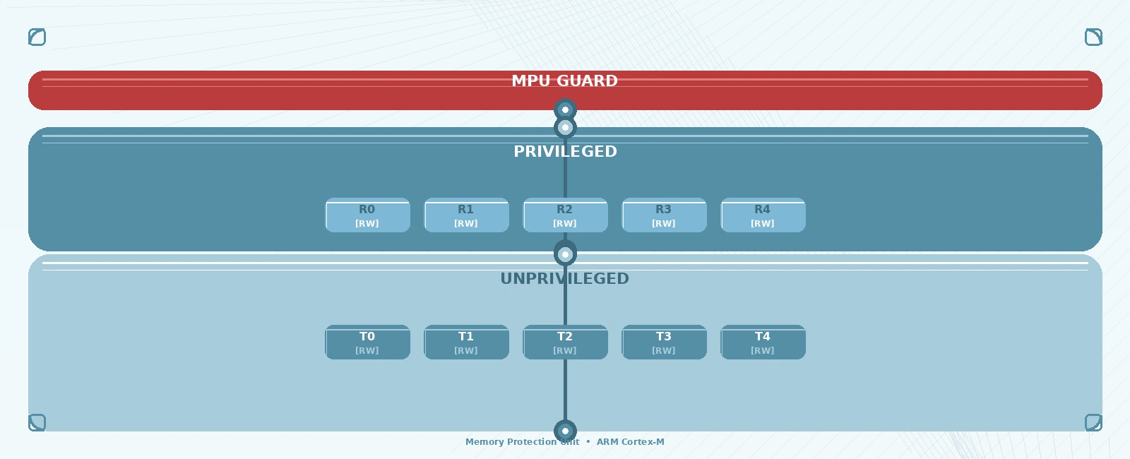
The ARM Cortex-M Memory Protection Unit (MPU) is the primary hardware mechanism for enforcing memory access policies in embedded systems. Unlike an MMU, it does not perform virtual-to-physical address translation — it simply checks every memory access against a set of programmer-defined regions and faults on violations. Proper MPU configuration is essential for privilege separation, stack overflow detection, execute-never enforcement, and safety-critical certification (IEC 61508, ISO 26262).
The MPU is programmed through a set of core registers accessed via the System Control Block (SCB):
| Register | Purpose |
|---|---|
MPU_TYPE | Read-only: number of instruction/data regions (DREGION, IREGION) |
MPU_CTRL | Global enable, HFNMIENA (enable during HardFault/NMI), PRIVDEFENA (default memory map for privileged) |
MPU_RNR | Region Number Register — selects which region to program |
MPU_RBAR | Region Base Address Register — base address (optionally with VALID + REGION fields in ARMv7-M, or with AP/XN/SH attributes in ARMv8-M) |
MPU_RASR | Region Attribute and Size Register (ARMv7-M only) — size, permissions, subregions, enable |
MPU_RLAR | Region Limit Address Register (ARMv8-M only) — upper bound + attributes |
Each region defines:
// ARMv7-M style (Cortex-M3/M4/M7)#define MPU_REGION_SIZE_32KB (14 << 1) // 2^(14+1) = 32KB#define MPU_REGION_ENABLE (1 << 0)void mpu_configure_region(uint8_t region, uint32_t base_addr,uint32_t size_attr, uint32_t access_attr) {SCB->MPU_RNR = region;SCB->MPU_RBAR = base_addr;SCB->MPU_RASR = size_attr | access_attr | MPU_REGION_ENABLE;}// ARMv8-M style (Cortex-M33/M55/M85) - uses RLAR for limit addressvoid mpu_configure_region_v8(uint8_t region, uint32_t base_addr, uint32_t rbar_attr,uint32_t limit_addr, uint32_t rlar_attr) {SCB->MPU_RNR = region;SCB->MPU_RBAR = base_addr | rbar_attr;SCB->MPU_RLAR = limit_addr | rlar_attr;}
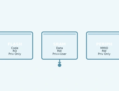
A production MPU configuration usually defines regions in priority order (higher region number = higher priority on overlap):
+---------------------------------------------------------------+| Region 7 (highest): PERIPHERALS - RW, XN, Device/nGnRnE || Region 6: FLASH (code) - RX, Privileged only || Region 5: FLASH (data/const) - R, Privileged || Region 4: KERNEL RAM - RW, XN, Privileged || Region 3: TASK A STACK - RW, XN, Unprivileged || Region 2: TASK B STACK - RW, XN, Unprivileged || Region 1: SHARED/IPC BUFFER - RW, XN, Both || Region 0 (lowest): BACKGROUND - Default map (PRIVDEFENA) |+---------------------------------------------------------------+
| AP[2:0] | Privileged | Unprivileged | Description |
|---|---|---|---|
| 000 | No access | No access | No access (faults) |
| 001 | RW | No access | Privileged only |
| 010 | RW | R | Privileged RW, Unprivileged R |
| 011 | RW | RW | Full access |
| 100 | — | — | Reserved |
| 101 | R | No access | Privileged R only |
| 110 | R | R | Read-only (both) |
| 111 | R | R | Read-only (both, alias) |
XN (Execute Never): Bit 28 in RASR. Always set XN=1 for RAM and peripheral regions.
| TEX[2:0] | S | C | B | Memory Type | Typical Use |
|---|---|---|---|---|---|
| 000 | x | 0 | 0 | Strongly Ordered | Peripherals, shared memory |
| 000 | x | 0 | 1 | Device (shared) | Memory-mapped peripherals |
| 001 | 0 | 0 | 0 | Normal, Outer/Inner Non-cacheable | Uncached RAM |
| 000 | 0 | 1 | 1 | Normal, Outer/Inner Write-Back | Cached RAM (with caution) |
| 010 | x | 0 | 0 | Device (non-shared) | Non-shared peripherals |
For most embedded code: Device/nGnRnE for peripherals, Normal Non-cacheable for RAM, Normal WT/WB for cacheable Flash.
Each region splits into 8 equal subregions. Setting a bit in SRD[7:0] disables that subregion:
// 64KB region at 0x2000_0000, disable subregions 2 and 3 (middle 16KB)// to carve out a hole for a peripheral mapped inside RAM spaceuint32_t srd = (1 << 2) | (1 << 3); // Disable subregions 2,3SCB->MPU_RASR |= (srd << 8);
Subregion disable is one technique for carving out address ranges with different permissions inside a larger region. The other is to use overlapping regions with higher region numbers, which take priority.
ARMv8-M adds significant improvements:
// ARMv8-M RLAR encoding#define MPU_RLAR_LIMIT_MASK (0xFFFFFFE0) // Limit address[31:5]#define MPU_RLAR_PXN (1 << 4) // Privileged Execute Never (v8.1-M)#define MPU_RLAR_ATTR_IDX(n) ((n) << 1) // MAIR index (0-7)#define MPU_RLAR_EN (1 << 0) // Region enable// MAIR programming (per attribute index)SCB->MAIR0 = (ATTR_DEVICE_nGnRnE << 0) | // Attr0: Device(ATTR_NORMAL_NC << 8) | // Attr1: Normal Non-cacheable(ATTR_NORMAL_WB << 16) | // Attr2: Normal Write-Back(ATTR_NORMAL_WT << 24); // Attr3: Normal Write-Through
void mpu_enable(void) {// 1. Disable MPU before configurationSCB->MPU_CTRL = 0;// 2. Configure all regions (as shown above)mpu_setup_regions();// 3. Enable MPU with:// - MPU_CTRL.ENABLE = 1// - MPU_CTRL.HFNMIENA = 1 (MPU active during HardFault/NMI)// - MPU_CTRL.PRIVDEFENA = 1 (Default memory map for privileged)SCB->MPU_CTRL = (1 << 0) | (1 << 1) | (1 << 2);// 4. DSB + ISB to ensure MPU takes effect before next instruction__DSB();__ISB();}
PRIVDEFENA=1: When MPU is enabled but no region matches, privileged accesses use the default memory map. Unprivileged accesses fault. This is the safe default.
Place a guard region immediately below each task stack:
// Task stack: 0x2000_8000 - 0x2000_9FFF (8KB)// Guard region: 0x2000_7000 - 0x2000_7FFF (4KB, No Access)#define STACK_TOP 0x2000A000#define STACK_SIZE 0x2000 // 8KB#define GUARD_SIZE 0x1000 // 4KB#define GUARD_BASE (STACK_TOP - STACK_SIZE - GUARD_SIZE)mpu_configure_region(REGION_STACK_GUARD,GUARD_BASE,MPU_REGION_SIZE_4KB | MPU_AP_PRIV_NO_UNPRIV_NO | MPU_XN,0); // No access for anyone
Any stack overflow into the guard region triggers a MemManage fault.
Every RAM and peripheral region must have XN=1. This prevents code injection attacks and catches accidental execution from data buffers.
// RAM region - RW, XN#define RASR_RAM (MPU_REGION_SIZE_64KB | MPU_AP_FULL | MPU_XN | MPU_TEX_SCB_NORMAL_NC)// Peripheral region - RW, XN, Device#define RASR_PERIPH (MPU_REGION_SIZE_512MB | MPU_AP_PRIV_ONLY | MPU_XN | MPU_TEX_SCB_DEVICE)
| Pitfall | Consequence | Fix |
|---|---|---|
| Region base not size-aligned | Unpredictable behavior / fault on config | Align base to region size (use __ALIGNED() or linker script) |
| Overlapping regions with wrong priority | Lower-priority region wins unexpectedly | Higher region number = higher priority. Plan region numbers carefully. |
| Forgetting XN on RAM | Code execution from data, security holes | Always set XN=1 for non-code regions |
| Subregion disable on ARMv8-M | SRD not supported in RLAR model | Use separate regions or MAIR attributes instead |
| MPU enabled before all regions configured | Default map gaps cause faults | Configure all regions, then enable in one atomic sequence |
| Not using HFNMIENA | MPU disabled during HardFault/NMI — debugger can’t inspect | Set HFNMIENA=1 for production; clear only for debug if needed |
void MemManage_Handler(void) {uint32_t mmfsr = SCB->CFSR & 0xFF; // MemManage Fault Status Registeruint32_t mmfar = SCB->MMFAR; // Faulting address (valid if MMARVALID=1)// MMFSR bits:// 0: IACCVIOL - Instruction access violation// 1: DACCVIOL - Data access violation// 3: MUNSTKERR - Unstacking error// 4: MSTKERR - Stacking error// 5: MLSPERR - Lazy FPU stacking error// 7: MMARVALID - MMFAR validlog_error("MemManage fault: %s%s%s",(mmfsr & 1) ? "IACCVIOL " : "",(mmfsr & 2) ? "DACCVIOL " : "",(mmfsr & 8) ? "MUNSTKERR " : "");if (mmfsr & (1 << 7)) {log_error("Faulting address: 0x%08X", mmfar);}// For RTOS: identify faulting task, dump context, trigger watchdog reset// Do NOT return from this handler if fault is unrecoverablewhile (1) { __WFI(); }}
| Aspect | ARMv7-M (M3/M4/M7) | ARMv8-M (M33/M55/M85) |
|---|---|---|
| Max regions | 8 | 16 |
| Size encoding | Power-of-2 (SIZE field) | Limit address (RLAR) |
| Permissions | AP[2:0] + XN | AP[1:0] (RO, NP) + XN (+ PXN in v8.1-M) |
| Memory attrs | TEX/S/C/B | MAIR[7:0] indices |
| Subregions | 8 per region (SRD) | Not supported (use regions) |
The MPU is not optional for robust embedded firmware. A well-designed MPU configuration catches stack overflows, prevents privilege escalation, enforces execute-never, and provides the hardware foundation for safety certification. Invest the time to map your memory, define regions carefully, and test every boundary.
Quick Links
Legal Stuff