


JTAG and SWD Debugging Strategies for Embedded Systems
June 11, 2026
4 min
Analog-to-Digital Converters (ADCs) are the bridge between the physical world and the digital domain in embedded systems. Whether you are measuring temperature, reading a microphone, monitoring battery voltage, or implementing a precision instrumentation system, the ADC is the critical component that determines how faithfully your system captures reality. Understanding ADC architecture, sampling theory, and practical design techniques is essential for any embedded engineer.
An ADC converts a continuous analog voltage into a discrete digital number. The conversion process involves three stages: sampling, quantization, and encoding. Sampling captures the analog signal at discrete time intervals. Quantization maps each sample to the nearest discrete level from a finite set. Encoding represents that level as a binary number.
The resolution of an ADC is defined by the number of bits in its output. A 12-bit ADC divides the input range into 2^12 = 4,096 discrete levels. For a 3.3V reference, each step represents 3.3V / 4096 ≈ 0.8 mV. A 16-bit ADC with the same reference achieves 3.3V / 65536 ≈ 0.05 mV per step — a 16x improvement in granularity.
+------------------------------------------------------------------+| ADC Conversion Pipeline |+------------------------------------------------------------------+| || Analog +-----------+ +-----------+ +-----------+ || Input ----->| Sample |--->| Quantize |--->| Encode |---->| Digital Out| Voltage | & Hold | | to N bits | | to Binary | || +-----------+ +-----------+ +-----------+ || || Continuous Discrete time Discrete levels Binary || voltage samples (2^N levels) code |+------------------------------------------------------------------+
The Nyquist-Shannon sampling theorem states that to accurately reconstruct a baseband signal, you must sample at a rate strictly greater than twice its highest frequency component. This minimum bound is called the Nyquist rate. If you sample below this rate, aliasing occurs — high-frequency components fold back into the measured bandwidth as false low-frequency signals.
In practice, sampling at exactly 2x the maximum signal frequency is insufficient. Real-world anti-aliasing filters cannot achieve an infinitely sharp cutoff, so for simple analog filters, engineers typically sample at 5x to 10x the maximum signal frequency. While audio applications (20 kHz bandwidth) output at 44.1 kHz or 48 kHz (only ~2.2x), they achieve this using Delta-Sigma ADCs that internally oversample at much higher frequencies (e.g., several MHz) to allow for gentle analog filtering, followed by sharp digital decimation filters.
+------------------------------------------------------------------+| Aliasing: What Happens When You Undersample |+------------------------------------------------------------------+| || Signal Sample Reconstructed || Freq Rate Freq Result || -------- ------- --------- -------------------------------- || 1 kHz 10 kHz 1 kHz OK - Correct reconstruction || 3 kHz 10 kHz 3 kHz OK - Below Nyquist freq (5 kHz) || 6 kHz 10 kHz 4 kHz X - Aliased! Folds to |Fin-Fs| || 8 kHz 10 kHz 2 kHz X - Aliased! Folds to |Fin-Fs| || 12 kHz 10 kHz 2 kHz X - Aliased! Folds to |Fin-Fs| || || Rule: Sample rate must be > 2x the highest signal frequency |+------------------------------------------------------------------+
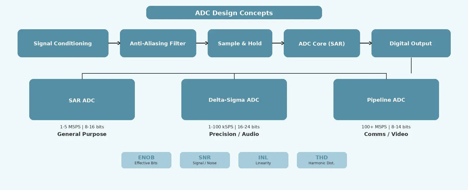
SAR ADCs are the most common architecture in microcontrollers. They use a binary search algorithm: the internal DAC generates a trial voltage, the comparator checks whether the input is above or below, and the logic narrows the range one bit per clock cycle. A 12-bit conversion requires 12 cycles for the successive approximation process, plus a programmable number of cycles for the initial sample-and-hold acquisition phase.
SAR ADCs offer an excellent balance of speed (up to several MSPS), resolution (8-16 bits), and power consumption. They are ideal for multiplexed multi-channel applications where the input switches between different signals between conversions.
Delta-Sigma ADCs use oversampling and noise shaping to achieve very high resolution (16-24 bits) at lower output data rates. They sample the input at a much higher internal rate (often MHz) and use a digital filter to decimate the data to the desired output rate. The key advantage is that they trade speed for resolution without requiring precision analog components.
These are the right choice for precision measurement applications: weigh scales, temperature sensors, and audio ADCs where 20+ effective bits of resolution matter more than raw throughput.
Pipeline ADCs use multiple low-resolution stages in series, each handling a few bits and passing the residual to the next stage. This architecture achieves very high sample rates (hundreds of MSPS to GSPS) at moderate resolution (8-14 bits). They are common in communications, radar, and video applications but are rarely integrated into general-purpose microcontrollers.
| Architecture | Speed | Resolution | Best For |
|---|---|---|---|
| SAR | 1-5 MSPS | 8-16 bits | General purpose, multiplexed channels |
| Delta-Sigma | 1-100 kSPS | 16-24 bits | Precision measurement, audio, sensors |
| Pipeline | 100+ MSPS | 8-14 bits | Communications, video, software-defined radio |
When selecting an ADC for an embedded design, several specifications determine whether it meets your requirements:
Effective Number of Bits (ENOB): The real-world resolution after accounting for noise and distortion. A 12-bit ADC with 10.5 ENOB performs like an ideal 10.5-bit ADC. Always check ENOB in the datasheet — it is often 1-2 bits less than the nominal resolution.
Signal-to-Noise Ratio (SNR): The ratio of the RMS signal amplitude to the RMS noise floor, expressed in dB. For an ideal N-bit ADC, SNR ≈ 6.02N + 1.76 dB. A perfect 12-bit ADC has an SNR of 74 dB.
Integral Non-Linearity (INL): The maximum deviation of the actual transfer function from a straight line, measured in LSBs. An INL of ±2 LSBs means the output code can be up to 2 counts away from the ideal value at any point in the range.
Differential Non-Linearity (DNL): The maximum deviation between two adjacent quantization steps from the ideal 1 LSB size. A DNL worse than -1 LSB can lead to “missing codes,” where a specific digital output value is never produced regardless of the analog input.
Total Harmonic Distortion (THD): The ratio of the sum of harmonic components to the fundamental frequency. Critical for audio and communication applications where harmonic spurs degrade signal quality.
Most MCU ADC inputs expect a 0V to VREF signal range. Real-world signals often need conditioning. A voltage divider scales down higher voltages. An op-amp buffer provides a low-impedance source, which is critical because the ADC’s internal sample-and-hold capacitor must charge to the input voltage within the sample time.
// Example: Reading a 0-12V battery through a voltage divider// Divider ratio: R1=10k, R2=3.3k => Vout = Vin * 3.3k / (10k + 3.3k)// At 12V input: Vout = 12 * (3.3 / 13.3) = 2.977V (within 3.3V reference)#define ADC_RESOLUTION 4096.0f // 12-bit ADC#define ADC_VREF 3.3f // Reference voltage#define DIVIDER_RATIO (3.3f / (10.0f + 3.3f)) // Let compiler calculate exact ratiofloat read_battery_voltage(uint16_t adc_raw){// Parentheses allow the compiler to pre-calculate the constant, saving a runtime divisionfloat adc_voltage = (float)adc_raw * (ADC_VREF / ADC_RESOLUTION);float battery_voltage = adc_voltage / DIVIDER_RATIO;return battery_voltage;}
If your signal has sufficient random white noise (at least 1 LSB of amplitude) and you do not need the full sample rate, oversampling and decimation can increase your effective resolution. While simple averaging reduces variance (noise), properly accumulating 4^n samples (ensuring your accumulator is a large enough variable, like uint32_t, to prevent overflow) and right-shifting by n (which is mathematically dividing by 2^n) yields n extra integer bits of resolution. Oversampling by 4 gains 1 extra bit. Oversampling by 16 gains 2 bits. This technique effectively trades CPU time, memory, and sample rate for resolution.
| Samples | SNR Gain | Extra Bits | Effective 12-bit ENOB |
|---|---|---|---|
| 1 | 0 dB | 0 bits | 12.0 bits |
| 4 | 6 dB | 1 bit | 13.0 bits |
| 16 | 12 dB | 2 bits | 14.0 bits |
| 64 | 18 dB | 3 bits | 15.0 bits |
| 256 | 24 dB | 4 bits | 16.0 bits |
Formula: ENOB_gain = 0.5 * log2(N)
For high-speed or continuous ADC sampling, using DMA eliminates CPU overhead. The ADC triggers a DMA request after each conversion, and the DMA controller transfers the result into a memory buffer. The CPU is only interrupted when the buffer is half-full or full, allowing efficient batch processing.
This approach is essential for applications like audio capture, vibration analysis, or any scenario where you need sustained sample rates above a few kHz without starving the application logic.
The ADC reference voltage determines the full-scale input range and directly impacts accuracy. Using the MCU’s internal reference (typically 1.2V to 3.3V) is convenient but may have poor initial accuracy (±1-3%) and temperature drift. For precision measurements, an external reference like the REF3030 (3.0V, ±0.15% initial accuracy, 25 ppm/C drift) provides a stable, known reference that improves absolute accuracy significantly.
ADC design in embedded systems requires understanding both the theoretical foundations (Nyquist criterion, quantization noise) and practical techniques (signal conditioning, averaging, DMA). SAR ADCs are the workhorse for general-purpose embedded applications, while Delta-Sigma ADCs excel in precision measurement. Always check ENOB rather than nominal resolution, condition your input signals properly, and use averaging or oversampling when you need extra resolution. With these concepts in hand, you can confidently select and implement ADCs for any embedded application.
Quick Links
Legal Stuff