


IEEE 1588 PTP Implementation on Embedded Systems
July 23, 2026
4 min
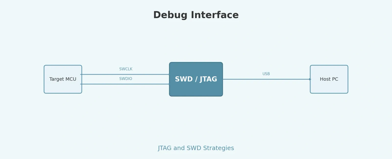
Debugging is one of the most critical skills in embedded systems development. Unlike desktop applications, embedded firmware runs on resource-constrained hardware with limited visibility into internal state. Two debug interfaces dominate the ARM Cortex-M ecosystem: JTAG (Joint Test Action Group) and SWD (Serial Wire Debug). Understanding their differences, trade-offs, and practical debugging strategies can dramatically improve your development workflow.
JTAG, standardized as IEEE 1149.1, has been the industry standard for decades. It uses a Test Access Port (TAP) controller with a state machine that shifts data through a scan chain. A typical JTAG connection requires four mandatory pins — TCK (clock), TMS (mode select), TDI (data in), and TDO (data out) — plus an optional TRST (reset). JTAG supports boundary scan testing, which is invaluable for PCB manufacturing tests and verifying interconnections between devices.
SWD, developed by ARM as part of the CoreSight debug architecture, is a two-pin alternative that provides the same debug capabilities as JTAG (minus boundary scan). It uses SWDIO (bidirectional data) and SWCLK (clock). Most modern Cortex-M MCUs implement a combined SWJ-DP (Serial Wire/JTAG Debug Port) that can auto-negotiate between the two protocols, sharing pins so that SWD signals overlay JTAG signals.
+----------------------------------------------------------+| Debug Interface Comparison |+---------------------------+------------------------------+| JTAG (IEEE 1149.1) | SWD (ARM CoreSight) |+---------------------------+------------------------------+| 4-5 pins (TCK,TMS,TDI, | 2 pins (SWDIO, SWCLK) || TDO, TRST) | |+---------------------------+------------------------------+| Boundary scan supported | No boundary scan |+---------------------------+------------------------------+| Up to ~20 MHz clock | Up to 30 MHz clock |+---------------------------+------------------------------+| TAP state machine | Packet-based protocol |+---------------------------+------------------------------+| Multi-device scan chain | Multi-drop (SWD v2) |+---------------------------+------------------------------+
For most Cortex-M microcontroller projects, SWD is the recommended default. The two-pin interface conserves precious GPIO pins — a critical consideration on small packages like QFN-32 or WLCSP. SWD also offers higher clock rates, which translates to faster flash programming and smoother stepping through code during debug sessions.
However, JTAG remains essential in several scenarios. If your design requires boundary scan testing for production PCB verification, JTAG is the only option. When debugging multi-processor SoCs with legacy ARM cores (ARM7, ARM9, ARM11) alongside Cortex-M cores, JTAG’s scan chain architecture allows a single debug probe to access all devices. Some older debug tools also only support JTAG.
A practical strategy is to design your board with a SWJ-DP compatible header that exposes both protocols. ARM recommends the 10-pin Cortex Debug Connector (0.05” pitch) for new designs — it supports SWD, JTAG, and Serial Wire Viewer (SWV) trace through a compact, low-cost connector.
ARM Cortex-M processors provide a Flash Patch and Breakpoint (FPB) unit that supports hardware breakpoints. The number of available breakpoints is implementation-defined — Cortex-M3/M4 devices typically provide 6 instruction comparators, while Cortex-M7 can support up to 8 (check your MCU’s FP_CTRL register for the exact count). These are essential for debugging code in flash memory since you can’t insert software breakpoint instructions (like BKPT) into read-only flash without the FPB remapping mechanism.
For data watchpoints, the Data Watchpoint and Trace (DWT) unit allows you to halt execution when a specific memory address is read or written. This is invaluable for tracking down stack overflows, buffer overruns, and unexpected peripheral register modifications.
// Example: Setting a data watchpoint on a variable using DWT// (Cortex-M4 with 4 comparators)volatile uint32_t sensor_value = 0;void enable_data_watchpoint(void){// Enable DWT and ITMCoreDebug->DEMCR |= CoreDebug_DEMCR_TRCENA_Msk;// Configure DWT comparator 0DWT->COMP0 = (uint32_t)&sensor_value; // Address to watchDWT->MASK0 = 0; // Match exact address (4 bytes)DWT->FUNCTION0 = 0x5; // Data read watchpoint (FUNCTION = 0b0101)// Now halt on debugger — any read of sensor_value triggers a halt}
Semihosting allows the target to use the debugger’s I/O facilities — for example, printing to the host console via printf. While convenient, semihosting is slow (it halts the CPU for each operation) and should be avoided in timing-sensitive code.
A better alternative is SWO (Serial Wire Output), which provides a dedicated trace pin for streaming data with minimal CPU overhead. Combined with the Instrumentation Trace Macrocell (ITM), SWO can output printf-style messages, data trace events, and exception entry/exit information without halting the target.
// ITM-based printf redirection via SWO (non-blocking)int _write(int file, char *ptr, int len){for (int i = 0; i < len; i++){ITM_SendChar(*ptr++);}return len;}// Usage: printf("Sensor: %d\r\n", sensor_value);// Output appears on SWO pin at core clock (HCLK) / (TPI->ACPR + 1)
HardFaults are among the most common and frustrating issues in embedded development. When a HardFault occurs, the processor pushes a stack frame containing the program counter (PC), link register (LR), R0–R3, R12, and xPSR. Additionally, the System Control Block (SCB) provides the Configurable Fault Status Register (CFSR) and fault address registers that indicate the fault cause.
A systematic approach to fault debugging:
// HardFault handler that captures diagnostic informationvoid HardFault_Handler(void){__asm volatile ("TST LR, #4 \n" // Check EXC_RETURN bit 2"ITE EQ \n""MRSEQ R0, MSP \n" // Use MSP if bit 2 == 0"MRSNE R0, PSP \n" // Use PSP if bit 2 == 1"B hard_fault_handler_c \n");}void hard_fault_handler_c(uint32_t *hardfault_args){volatile uint32_t stacked_pc = hardfault_args[6];volatile uint32_t stacked_lr = hardfault_args[5];volatile uint32_t cfsr = SCB->CFSR;volatile uint32_t bfar = SCB->BFAR;volatile uint32_t mmfar = SCB->MMFAR;// Set a breakpoint here in your debugger to inspect these values(void)stacked_pc;(void)stacked_lr;(void)cfsr;(void)bfar;(void)mmfar;while (1) { }}
Modern embedded designs increasingly use multi-core MCUs (e.g., Cortex-M4 + Cortex-M0+). SWD version 2 introduces Multi-Drop, allowing a single debug probe to access multiple DAPs (Debug Access Ports) on the same SWD bus. Each DAP has a unique target ID, and the debugger selects which core to communicate with using a target selection protocol.
For JTAG-based multi-core debugging, devices are daisy-chained in a scan chain. The debugger must know the position and instruction register length of each device in the chain — typically configured via a board description file (like a .jtag or .svf file).
The choice of debug probe significantly impacts your debugging experience. Popular options include:
| Probe | Protocols | Speed | Notes |
|---|---|---|---|
| SEGGER J-Link | JTAG + SWD | Up to 50 MHz | Industry standard, excellent IDE integration |
| CMSIS-DAP / DAPLink | JTAG + SWD | Up to 10 MHz | Open source, no drivers needed (USB HID) |
| ST-LINK/V3 | JTAG + SWD | Up to 24 MHz | Bundled with STM32 Nucleo/Discovery boards |
| ULINKpro | JTAG + SWD | Up to 50 MHz | ARM/KEIL, supports ETM trace (100 MHz trace clock) |
For professional development, SEGGER J-Link offers the best combination of speed, reliability, and tool integration. For hobbyist or educational use, CMSIS-DAP based probes (often built into development boards) provide a zero-cost, driver-free solution.
Effective embedded debugging requires understanding both the hardware interfaces (JTAG vs SWD) and the architectural debug features built into your target processor. SWD is the practical choice for most Cortex-M projects due to its lower pin count and higher speed, while JTAG remains necessary for boundary scan and legacy device support. Leveraging hardware breakpoints, ITM/SWO trace, and systematic fault analysis techniques will help you diagnose issues faster and ship more reliable firmware.
Quick Links
Legal Stuff