


Fixing I2C Clock Stretching Timeouts on STM32
July 07, 2026
3 min
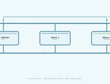
I²C (Inter-Integrated Circuit) is a synchronous, half-duplex serial communication protocol that has become ubiquitous in embedded systems due to its simplicity and efficiency. Using only two wires—SDA (Serial Data) and SCL (Serial Clock)—I²C enables multiple devices to communicate on the same bus, making it ideal for connecting sensors, EEPROMs, real-time clocks, and other peripherals to microcontrollers.
In embedded systems where pin count and board space are at a premium, I²C offers significant advantages over alternatives like SPI and UART. Unlike SPI, which requires a separate chip select line for each device, I²C uses device addressing to allow multiple peripherals to share the same two-wire bus. Compared to UART, I²C eliminates the need for pre-agreed baud rates and start/stop bits per byte, reducing protocol overhead.
The protocol supports both single-controller and multi-controller configurations, with built-in arbitration to resolve bus contention when multiple controllers attempt to communicate simultaneously. Standard I²C operates at 100 kHz (standard mode) or 400 kHz (fast mode), with optional higher-speed modes available for applications requiring faster data transfer.
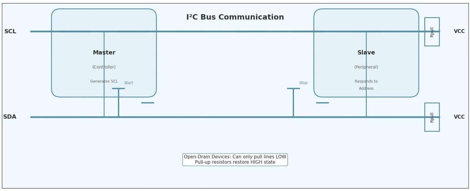
I²C communication relies on just two bidirectional open-drain lines:
The open-drain design is crucial to I²C’s robustness. Each device can only pull the bus lines low; it cannot drive them high. External pull-up resistors (typically 4.7kΩ) restore the lines to their high state when no device is actively pulling them low. This prevents bus contention—if two devices attempt to drive the bus simultaneously, there’s no risk of damage from conflicting high/low drives.
Logic level flexibility is another benefit. Since devices never drive the bus high, it’s possible to mix different voltage levels (e.g., 5V and 3.3V devices) on the same bus, provided the pull-up voltage is compatible with all connected devices.
I²C communication is structured around frames and special bus conditions:
Every I²C transaction begins with a Start Condition and ends with a Stop Condition:
These conditions are uniquely identifiable because, during normal data transfer, SDA only changes state when SCL is low. This ensures Start and Stop conditions are never mistaken for regular data bits.
Each byte transmitted on the I²C bus is followed by a ninth clock pulse during which the receiver sends an ACK (acknowledge) or NACK (not acknowledge) bit:
The transmitter monitors the ACK/NACK bit to confirm successful reception. If a NACK is received, the transmitter knows the operation failed and should terminate the transaction with a Stop Condition.
The most frequent I²C operation involves writing data to a slave device’s register:
The slave device acknowledges each byte received. If the slave NACKs any byte, the master should abort the transaction.
Reading requires a slightly more complex sequence known as a “combined format”:
The Repeated Start Condition is essential here—it allows the master to retain bus control between writing the register address and reading the data, preventing another master from intervening.
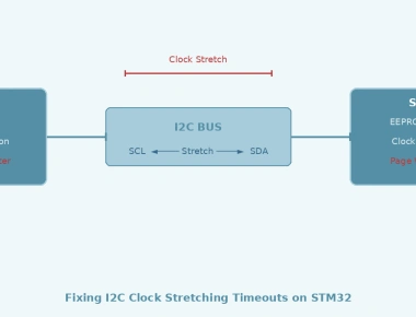
Slave devices can hold the SCL line low after the master releases it to request additional time for processing (e.g., completing an analog-to-digital conversion or finishing an EEPROM write operation). The master must detect this condition and wait until the slave releases the clock line before continuing. This feature allows slower slaves to communicate with faster masters without data loss.
In multi-controller systems, arbitration determines which master gains control of the bus when two or more attempt to initiate communication simultaneously. The process is non-destructive:
This ensures bus integrity even when multiple controllers compete for access.
Choosing appropriate pull-up resistor values is critical for reliable I²C communication:
The I²C specification limits total bus capacitance to 400pF for standard mode and faster modes. Excessive capacitance slows rise times, potentially causing timing violations. Keep bus traces short and use proper PCB layout techniques to minimize capacitance.
Ensure all devices on the bus have unique addresses. Some devices have fixed addresses, while others allow address selection via pins. Check device datasheets carefully to avoid conflicts, especially when using multiple instances of the same component.
In electrically noisy environments:
The most common I²C issue is missing or incorrectly sized pull-up resistors, resulting in sluggish or non-functional communication. Always verify pull-ups are present and appropriately sized for your bus configuration.
Generating Start or Stop conditions at the wrong time can confuse devices on the bus. Remember that these conditions are defined by specific SDA transitions while SCL is high—a state that never occurs during normal data transfer.
Masters that don’t account for clock stretching may read incorrect data or cause slave devices to malfunction. Always implement timeout mechanisms when waiting for the clock line to be released.
Long wires or excessive PCB trace capacitance can degrade signal quality, particularly at higher speeds. Measure bus capacitance if experiencing intermittent communication issues.
I²C remains a cornerstone of embedded systems communication due to its elegant simplicity, multi-device capability, and robust error handling. Its two-wire interface minimizes pin usage while supporting complex multi-controller systems through built-in arbitration. The protocol’s design—featuring open-drain lines, acknowledgment bits, and well-defined start/stop conditions—provides a reliable foundation for communication between microcontrollers and peripheral devices.
When properly implemented with appropriate pull-up resistors, attention to bus capacitance, and awareness of advanced features like clock stretching and repeated start conditions, I²C enables flexible, scalable designs suitable for everything from simple sensor networks to complex multi-processor systems. Understanding these fundamentals allows embedded engineers to leverage I²C’s full potential while avoiding common implementation pitfalls.
Quick Links
Legal Stuff