

Effective Embedded Firmware Code Review Checklist
September 03, 2026
9 min
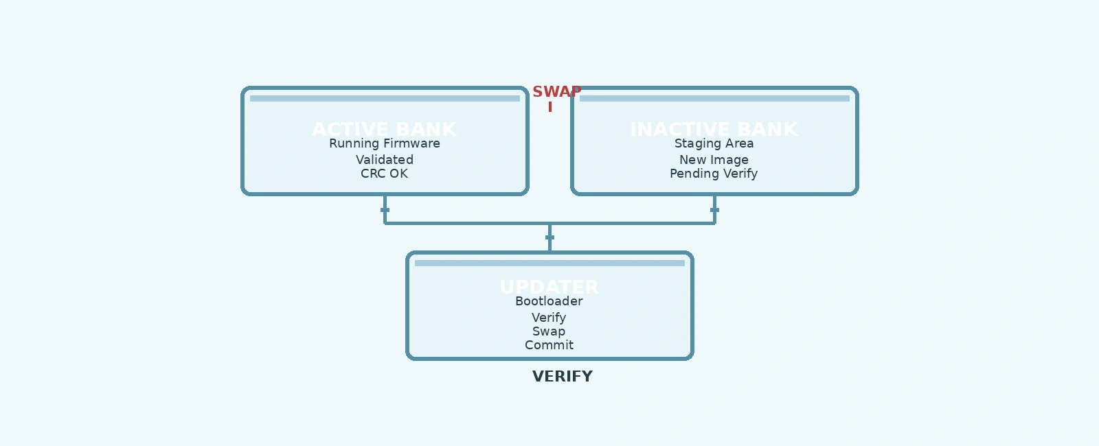
Firmware updates are a critical lifecycle operation for connected and mission-critical embedded devices. The architectural choice between A/B (dual bank / active-inactive) and in-place (single bank / staged) update strategies fundamentally dictates system availability, memory layout, power-loss resilience, and recovery mechanisms.
This article examines the underlying hardware constraints, memory architectures, rollback state machines, and cryptographic verification pipelines for both approaches.
Understanding update mechanisms requires examining the physical behavior of microcontroller NOR flash:
BusFault / HardFault.1) to a programmed state (0). Rewriting requires an erase operation at sector/block granularity (typically 2 KB to 128 KB). Partial writes or state-flag updates must account for minimum write granularities (word / double-word) and flash error-correcting code (ECC) restrictions.In an A/B architecture, non-volatile memory is divided into two symmetrical application partitions (Bank A and Bank B) alongside a protected bootloader and shared metadata storage. One bank executes the active runtime while the second bank acts as an inactive staging slot.
+----------------------------------------------------------------------------+| Dual-Bank Flash Memory Map |+---------------------+---------------------+--------------------------------+| Base Address | Region Name | Description |+---------------------+---------------------+--------------------------------+| 0x08000000 | Bootloader (BL) | Immutable / Protected Bootcode || 0x08010000 | Metadata Ping-Pong | 2x Sectors (NVRAM State Logs) || 0x08020000 | Bank A (Slot 0) | Primary Application Partition || 0x080A0000 | Bank B (Slot 1) | Secondary Staging Partition |+---------------------+---------------------+--------------------------------+
+----------------------------------------------------------------------------+| A/B (Dual Bank) Update Flow |+----------------------------------------------------------------------------+| BOOTLOADER |+----------------------------------------------------------------------------+| 1. Power-on reset & clock initialization || 2. Read boot metadata record (Ping-Pong NVRAM sectors) || 3. Evaluate state machine: CONFIRMED vs. TESTING (Trial Boot) || 4. If state == TESTING && attempts == 0 -> ROLLBACK to previous bank || 5. Verify cryptographic signature (ECDSA-P256 / SHA-256) of target bank || 6. Relocate VTOR, initialize MSP, branch to target Reset_Handler |+----------------------------------------------------------------------------+|v+----------------------------------------------------------------------------+| APPLICATION RUNTIME (ACTIVE BANK) |+----------------------------------------------------------------------------+| 1. Normal operation (zero downtime during background download) || 2. Stream new firmware image into INACTIVE bank || 3. Authenticate image manifest & verify digital signature in inactive slot || 4. Write boot metadata: state = TESTING, attempts = 3, target = inactive || 5. Trigger software reset (NVIC_SystemReset) |+----------------------------------------------------------------------------+|v+----------------------------------------------------------------------------+| TRIAL BOOT & CONFIRMATION PHASE |+----------------------------------------------------------------------------+| 1. Bootloader boots new bank on probation (decrements attempts counter) || 2. New application boots, initializes drivers, and runs self-tests (POST) || 3. On successful self-test -> Application calls confirm_firmware_update() || 4. Metadata permanently committed: state = CONFIRMED || || [FAILURE PATH: Watchdog timeout or crash before confirmation] || -> Hardware reset triggers -> attempts == 0 -> Bootloader rolls back to A |+----------------------------------------------------------------------------+
.+--------------------------------+| STATE_CONFIRMED || (Bank A Active & Valid) |+--------------------------------+|OTA Payload Written to Bank BMetadata: state = TESTING, N = 3|v+------------+ Trial Boot N > 0 +--------------------------------+| WATCHDOG | <--------------------- | STATE_TESTING || CRASH LOOP | | (Bank B Trial Probation) |+------------+ +--------------------------------+| || N == 0 (Exhausted) | Self-Tests Passv | confirm_firmware_update()+--------------------------------+ v| ROLLBACK TO BANK A | +--------------------------------+| (Mark Bank A Confirmed) | | STATE_CONFIRMED |+--------------------------------+ | (Bank B Active & Valid) |+--------------------------------+
In-place updating overwrites the existing application partition with the new image. Because a running MCU cannot execute code from a flash sector it is actively erasing, in-place updates must be executed from an isolated execution environment.
+----------------------------------------------------------------------------+| Single-Bank Flash Memory Map |+---------------------+---------------------+--------------------------------+| Base Address | Region Name | Description |+---------------------+---------------------+--------------------------------+| 0x08000000 | Bootloader (BL) | Write-Protected DFU / Flasher || 0x08010000 | Boot Flags | Update Request Flags in NVRAM || 0x08020000 | Application Space | Single Overwritten Active App || (External SPI Flash)| Staging Slot | Golden Download Image Buffer |+---------------------+---------------------+--------------------------------+
+----------------------------------------------------------------------------+| In-Place Staged / RAM Update Flow |+----------------------------------------------------------------------------+| BOOTLOADER |+----------------------------------------------------------------------------+| 1. Power-on reset & hardware initialization || 2. Check for pending update flag in NVRAM || 3. If NO update: Verify current application signature and jump || 4. If UPDATE pending: Read staging buffer (external Flash / UART / USB) || 5. Erase application flash sectors || 6. Program new image into application space || 7. Verify new image digital signature || 8. Clear update flag and branch to application |+----------------------------------------------------------------------------+|v+----------------------------------------------------------------------------+| FAILURE MODES & RECOVERY CONSIDERATIONS |+----------------------------------------------------------------------------+| Power loss during erase/program leaves flash invalid. || Recovery requires: || - Write-protected Bootloader with fallback recovery agent (UART/USB DFU) || - Dedicated external storage holding the golden staging image || - Hardware Root-of-Trust ROM bootloader fallback |+----------------------------------------------------------------------------+
.ramfunc): If no external flash exists and the payload is streamed directly over a communication interface, the application copies its entire flashing routine, vector table, and communication stack to internal SRAM. Interrupts are disabled (__disable_irq()), instruction caches are invalidated, and execution transitions completely to SRAM before erasing internal Flash.| Metric / Dimension | A/B (Dual Bank) | In-Place (Single Bank Staged) | Swap-Scratch (MCUBoot Style) |
|---|---|---|---|
| Flash Memory Overhead | 2 × App Size + Bootloader | 1 × App Size + Bootloader | 2 × App Size + 1 Scratch Sector |
| Execution Address | Relocated / Dynamic / HW Alias | Static (Fixed Base Address) | Static (Always Slot 0) |
| Rollback Capability | Instantaneous & Atomic | No native rollback | Automatic physical two-way swap |
| Power-Loss Resilience | Highest (Old image remains intact) | Low (Requires DFU/ROM recovery) | High (Transaction log in Scratch) |
| System Availability | Zero downtime during download | Downtime during staging/flashing | Downtime during boot swap cycle |
| Flash Wear Distribution | Distributed evenly across banks | Concentrated on single app bank | High write amplification on Scratch |
| Linker Complexity | Moderate (PIC / Aliasing / Multi-target) | Low (Fixed memory layout) | Low (Single link address) |
| Standard Compliance | NIST SP 800-193, RFC 9019 (SUIT) | Maintenance / Factory only | PSA Certified Level 1–3, Zephyr |
Microcontroller binaries compiled for ARM Cortex-M or RISC-V contain absolute memory references (literal pools, interrupt vector tables, jump tables, and static variable initializers). If Bank A is at 0x08020000 and Bank B is at 0x080A0000, a binary linked for Bank A will crash if executed from Bank B unless addressed by one of the following architectures:
+----------------------------------------------------------------------------+| Address Resolution Architecture Options |+----------------------------------------------------------------------------+| 1. Hardware Dual-Bank Aliasing: || MCU option bits (e.g., STM32 SWP_FB) swap physical bank address || mapping. Active bank is ALWAYS mapped to 0x08000000. Binaries linked to || single address. || || 2. Swap-Scratch Physical Move (MCUBoot): || Slot 1 is download-only. Bootloader swaps Slot 1 -> Slot 0 block by || block. Application always executes from fixed Slot 0 address. || || 3. Position-Independent Code (PIC / ROPI / RWPI): || GCC flags -fPIC -mropi -mrwpi access code and constants via offset || tables. Eliminates fixed address dependencies with minimal overhead. || || 4. Asymmetric Dual-Target Compilation: || Build system outputs two distinct binaries: app_bank_a.bin and || app_bank_b.bin. Server distributes artifact matching target bank. |+----------------------------------------------------------------------------+
The following reference implementation implements a robust state machine with trial boot probation, watchdog crash-loop detection, Vector Table Offset Register (VTOR) relocation, and stack pointer initialization.
#include <stdint.h>#include <stdbool.h>#define BOOT_MAGIC_VALID 0x53544154 // 'STAT'#define MAX_TRIAL_BOOT_ATTEMPTS 3 // Used by application-side scheduling#define BANK_A_BASE 0x08020000U#define BANK_B_BASE 0x080A0000Utypedef enum {BANK_STATE_CONFIRMED = 0xAA,BANK_STATE_TESTING = 0x55,} bank_state_t;typedef struct {uint32_t magic;uint32_t sequence_num;uint8_t active_bank; // 0: Bank A, 1: Bank Buint8_t state; // bank_state_tuint8_t attempts_remaining; // Decremented on each trial bootuint8_t reserved;uint32_t crc32;} __attribute__((packed)) boot_metadata_t;// Forward declarations for platform HAL & security functionsextern bool nvram_read_metadata(boot_metadata_t *meta);extern bool nvram_write_metadata(const boot_metadata_t *meta);extern bool crypto_verify_bank_signature(uint8_t bank);extern void enter_recovery_dfu_mode(void);static void jump_to_application(uint8_t bank) {uint32_t bank_address = (bank == 0) ? BANK_A_BASE : BANK_B_BASE;uint32_t *vector_table = (uint32_t *)bank_address;// 1. Disable all interrupts and reset SysTick__disable_irq();SysTick->CTRL = 0;SysTick->LOAD = 0;SysTick->VAL = 0;// 2. Relocate Vector Table Offset Register (VTOR)SCB->VTOR = bank_address;// 3. Extract Initial Main Stack Pointer (MSP) and Reset Vectoruint32_t app_msp = vector_table[0];uint32_t app_reset = vector_table[1];// 4. Set MSP and branch to application Reset_Handler__set_MSP(app_msp);((void (*)(void))app_reset)();}void bootloader_main(void) {boot_metadata_t meta;if (!nvram_read_metadata(&meta) || meta.magic != BOOT_MAGIC_VALID) {// Uninitialized or corrupt metadata: default to Bank Ameta.magic = BOOT_MAGIC_VALID;meta.sequence_num = 1;meta.active_bank = 0;meta.state = BANK_STATE_CONFIRMED;meta.attempts_remaining = 0;nvram_write_metadata(&meta);}// Evaluate Trial Boot Probation Stateif (meta.state == BANK_STATE_TESTING) {if (meta.attempts_remaining > 0) {// Decrement remaining attempts and persist before launchingmeta.attempts_remaining--;nvram_write_metadata(&meta);} else {// Watchdog or panic reset loop occurred during trial: ROLLBACKmeta.active_bank = !meta.active_bank;meta.state = BANK_STATE_CONFIRMED;meta.attempts_remaining = 0;nvram_write_metadata(&meta);}}// Cryptographic Authenticity & Integrity Verification (ECDSA-P256 / SHA-256)if (!crypto_verify_bank_signature(meta.active_bank)) {// Target bank failed cryptographic verification; attempt fallback bankmeta.active_bank = !meta.active_bank;meta.state = BANK_STATE_CONFIRMED;nvram_write_metadata(&meta);if (!crypto_verify_bank_signature(meta.active_bank)) {// Both banks invalid: Enter safe recovery / DFU modeenter_recovery_dfu_mode();}}jump_to_application(meta.active_bank);}
Once the newly updated firmware boots, initializes peripherals, and confirms network or operational stability, it commits the update to permanent status:
void confirm_firmware_update(void) {boot_metadata_t meta;if (nvram_read_metadata(&meta)) {if (meta.state == BANK_STATE_TESTING) {meta.state = BANK_STATE_CONFIRMED;meta.attempts_remaining = 0;meta.sequence_num++;nvram_write_metadata(&meta);}}}
When updating in-place without a secondary bank, the erase and write routine must be linked to SRAM to avoid instruction fetch stalls on the internal flash bus:
// Placed in RAM section via compiler attribute__attribute__((section(".ramfunc"), noinline))bool execute_inplace_flash_from_ram(uint32_t flash_dst, const uint8_t *src_buf, size_t len) {// 1. Critical section: disable all global interrupts__disable_irq();// 2. Invalidate instruction and data caches if supported#if defined(SCB_ICSR)SCB_InvalidateICache();#endif// 3. Unlock flash controller peripheralFLASH->KEYR = FLASH_KEY1;FLASH->KEYR = FLASH_KEY2;// 4. Erase sectors across target application rangefor (uint32_t addr = flash_dst; addr < (flash_dst + len); addr += FLASH_SECTOR_SIZE) {if (internal_flash_erase_sector_ram(addr) != FLASH_SUCCESS) {FLASH->CR |= FLASH_CR_LOCK;return false; // Flash hardware fault}}// 5. Program new payload wordsfor (size_t offset = 0; offset < len; offset += FLASH_WRITE_UNIT) {if (internal_flash_write_word_ram(flash_dst + offset, *(const uint32_t *)(src_buf + offset)) != FLASH_SUCCESS) {FLASH->CR |= FLASH_CR_LOCK;return false;}}// 6. Lock flash controller and trigger system resetFLASH->CR |= FLASH_CR_LOCK;NVIC_SystemReset();return true; // Never reached}
For research and production environments compliant with NIST SP 800-193 and IETF RFC 9019 (SUIT), firmware update pipelines must enforce the following security controls:
+----------------------------------------------------------------------------+| Cryptographic Verification & Integrity Pipeline |+----------------------------------------------------------------------------+| 1. Manifest Validation: Parse signed header (image size, target HW ID). || 2. Signature Verification: Verify ECDSA P-256 / Ed25519 signature over || SHA-256 image digest using Root of Trust (RoT) Public Key in OTP/eFuse. || 3. Anti-Rollback Protection: Verify manifest security version counter || >= hardware monotonic counter. Update eFuse counter on commit. || 4. Decryption (Optional): Decrypt payload using AES-128/256-GCM. |+----------------------------------------------------------------------------+
.+-------------------------------+| Flash Budget >= 2x App Size? |+-------------------------------+|+--------------+--------------+YES NO| |+-----------------------------+ +-----------------------------+| Unattended OTA / Field? | | External Flash Available? |+-----------------------------+ +-----------------------------+| | | |YES NO YES NO| | | |v v v v+-------------+ +-------------+ +-------------+ +-------------+| A/B DUAL | | SINGLE-BANK | | IN-PLACE | | RAM-STAGED || BANK | | COST-OPTIM. | | EXT-STAGING | | FLASHER+DFU |+-------------+ +-------------+ +-------------+ +-------------+
Quick Links
Legal Stuff