

Fixing Zephyr Deep Sleep Backup SRAM Retention on STM32
September 12, 2026
4 min
PWM dead-time insertion is the silent killer of motor drive reliability. You configure the registers, the motor spins, and everything looks fine — until a thermal event or load transient reveals the MOSFETs are silently destroying each other through shoot-through. This article walks through the root causes, calculation methods, hardware implementation on STM32, and bench verification techniques that separate working drives from future field failures.
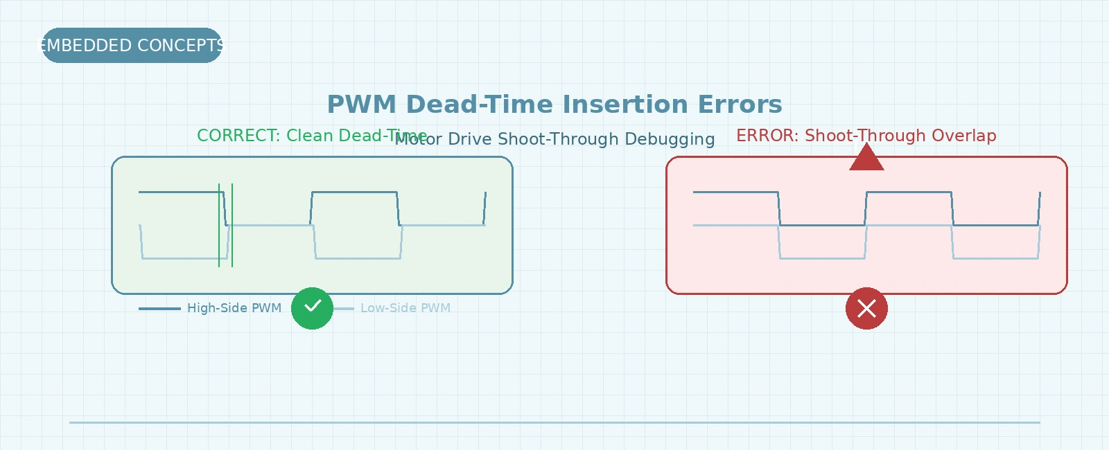
Every three-phase motor drive uses half-bridge legs — a high-side and low-side MOSFET switching a common phase node. The fundamental rule: never allow both devices to conduct simultaneously. When they do, the DC bus shorts directly through the two MOSFETs. This is shoot-through.
+------------------ DC Bus (+) ------------------+| || Drain || +-------+ || Gate_H ------> | QH | High-Side MOSFET || +-------+ || Source || | || +-----> Phase Node (U/V/W) || | (Motor Phase) || Drain || +-------+ || Gate_L ------> | QL | Low-Side MOSFET || +-------+ || Source || | || +-------+ || | R_sh | Current Shunt || +-------+ || | |+------------------ DC Bus (-) ------------------+
Shoot-through current is limited only by MOSFET Rds(on), PCB trace resistance, and bus capacitance ESR. In a 48V system with 5 mOhm total loop resistance, that is a theoretical peak of 9.6 kA — limited in practice by stray loop inductance to several hundred amperes for tens of nanoseconds. Even brief pulses generate severe localized die heating, vaporize bond wires, crack package encapsulation, and guarantee premature field returns.
The dead-time gap is the enforced delay between commanding one MOSFET off and commanding the complementary device on. It must guarantee that the departing device’s channel is completely extinguished and its gate charge dissipated before the arriving device begins conducting.
MOSFET datasheets specify turn-on (t_d(on)) and turn-off (t_d(off)) delays at 25°C, with minimal gate resistance (often 0 Ohm or 1 Ohm), and stiff lab gate power supplies. Production designs introduce critical deviations:
dv/dt control (10 Ohm to 47 Ohm typical)V_th) that drops with temperature (typically -3 mV/°C to -5 mV/°C)At 125°C junction temperature, a reduced V_th causes the turning-on MOSFET to conduct earlier in its gate voltage ramp, while the turning-off MOSFET takes longer to discharge below V_th. The dead-time margin calculated at room temperature quickly vanishes.
Half-bridge gate drivers exhibit timing asymmetry between high-side and low-side channels, as well as between turn-on and turn-off propagation paths (t_PLH vs t_PHL). Typical propagation delay mismatch (Delta_t_PDD) ranges from 15 ns to 50 ns across temperature and production lots. When using symmetrical dead-time insertion, the transition direction with the longer turn-off propagation delay suffers reduced margin.
The gate drive loop (gate driver output pin, gate trace, gate resistor, MOSFET gate, source pin, and ground return) forms an RLC resonant circuit with the MOSFET input capacitance (C_iss). Common-source inductance (L_S) in non-Kelvin packages slows down gate charging and discharging due to the opposing induced voltage V_Ls = L_S * (di/dt).
Furthermore, high dv/dt on the switching phase node couples capacitive current into the off-state MOSFET gate through the reverse transfer capacitance (C_rss / C_gd):
I_Miller = C_gd * (dv_ds / dt)
If the gate driver sink impedance plus trace resistance cannot shunt this current rapidly, the gate voltage spikes above V_th, causing cross-conduction during the dead-time window.
High-side bootstrap circuits rely on a floating capacitor refreshed exclusively during low-side conduction. At high duty cycles (>90%) or prolonged high-side on-states, the bootstrap capacitor voltage droops due to gate leakage, quiescent driver current, and bootstrap diode reverse recovery. Lower gate-source voltage increases high-side R_ds(on) and lengthens switching transitions, distorting calculated timing margins.
When an inductive load forces freewheeling current through the low-side MOSFET body diode during dead-time, minority carriers accumulate in the p-n junction. When the high-side MOSFET subsequently turns on, the body diode cannot block voltage instantly; it conducts reverse recovery current (I_rrm) while sweeping out stored charge (Q_rr). This creates a steep current spike and extreme phase-node dv/dt that exacerbates Miller-induced spurious turn-on.
Modern microcontrollers integrate dedicated hardware dead-time generators into advanced motor control timer peripherals. These modules operate synchronously with the timer kernel clock, providing deterministic, sub-nanosecond to single-nanosecond resolution independent of CPU execution or interrupt latency.
| MCU Family | Peripheral | Dead-Time Clock / Resolution | Channels |
|---|---|---|---|
| STM32F4/H7/G4 | TIM1 / TIM8 / TIM20 | t_DTS (up to 4.7 ns @ 212 MHz TIM_KER_CK) | 3 to 4 complementary pairs |
| STM32G474 / H7 | HRTIM (High-Res Timer) | Independent rising/falling down to 184 ps | 5 to 6 complementary pairs |
| TI C2000 (F28004x/F2837x) | ePWM Dead-Band (DB) | 1 / SYSCLK (down to ~10 ns, or MEP sub-ns) | 6 to 12 half-bridge pairs |
| NXP LPC55 / S32K3 / i.MX RT | eFlexPWM / SCTimer | 1 / BusClock (up to 5 ns @ 200 MHz) | 4 to 8 complementary pairs |
| Infineon XMC4000 / AURIX | CCU8 | 1 / f_CCU8 (down to 3.3 ns @ 150 MHz) | 4 dual-channel slices |
| Microchip dsPIC33CK | High-Speed PWM | 1 / (2 * F_PCO) (down to 250 ps) | 8 complementary pairs |
STM32 Advanced Timer Dead-Time Configuration (TIM1 on STM32G4/H7):
// STM32 TIM1 complementary PWM configuration with hardware dead-time insertion// Target: 100 kHz PWM, 150 ns dead-time on STM32G474 (TIM_KER_CK = 170 MHz -> t_tim = 5.88 ns)// DTG calculation: 150 ns / 5.88 ns = 25.5 -> 26 ticks (DTG[7:0] = 0x1A)TIM_BreakDeadTimeConfigTypeDef bdtr = {0};bdtr.OffStateRunMode = TIM_OSSR_ENABLE; // Drive inactive outputs in Run modebdtr.OffStateIDLEMode = TIM_OSSI_ENABLE; // Drive inactive outputs in Idle/Breakbdtr.LockLevel = TIM_LOCKLEVEL_OFF;bdtr.DeadTime = 26; // 26 ticks * 5.88 ns = 152.9 nsbdtr.BreakState = TIM_BREAK_ENABLE; // Hardware overcurrent trip via BKIN pinbdtr.BreakPolarity = TIM_BREAKPOLARITY_LOW;bdtr.BreakFilter = 0x3;bdtr.AutomaticOutput = TIM_AUTOMATICOUTPUT_ENABLE;if (HAL_TIMEx_ConfigBreakDeadTime(&htim1, &bdtr) != HAL_OK) {Error_Handler();}// Configure complementary PWM Channel 1 (U phase)TIM_OC_InitTypeDef oc = {0};oc.OCMode = TIM_OCMODE_PWM1;oc.Pulse = (htim1.Init.Period + 1) / 2; // 50% duty cycleoc.OCPolarity = TIM_OCPOLARITY_HIGH;oc.OCNPolarity = TIM_OCNPOLARITY_HIGH;oc.OCIdleState = TIM_OCIDLESTATE_RESET; // Low in idle/faultoc.OCNIdleState = TIM_OCNIDLESTATE_RESET; // Low in idle/faultoc.OCFastMode = TIM_OCFAST_DISABLE;HAL_TIM_PWM_ConfigChannel(&htim1, &oc, TIM_CHANNEL_1);HAL_TIM_PWM_ConfigChannel(&htim1, &oc, TIM_CHANNEL_2);HAL_TIM_PWM_ConfigChannel(&htim1, &oc, TIM_CHANNEL_3);// Start main and complementary channel outputsHAL_TIM_PWM_Start(&htim1, TIM_CHANNEL_1);HAL_TIMEx_PWMN_Start(&htim1, TIM_CHANNEL_1);HAL_TIM_PWM_Start(&htim1, TIM_CHANNEL_2);HAL_TIMEx_PWMN_Start(&htim1, TIM_CHANNEL_2);HAL_TIM_PWM_Start(&htim1, TIM_CHANNEL_3);HAL_TIMEx_PWMN_Start(&htim1, TIM_CHANNEL_3);// CRITICAL: Advanced timers (TIM1/TIM8/TIM20) require Main Output Enable (MOE)// Without setting MOE, outputs remain clamped to inactive state__HAL_TIM_MOE_ENABLE(&htim1);
Key STM32 registers: TIMx_BDTR.DTG[7:0] configures the dead-time interval, while TIMx_BDTR.MOE enables the output stages. The dead-time encoding uses non-linear piecewise ranges for values above 127.
General-purpose timers (such as STM32 TIM2-TIM5) lack complementary output circuitry and the BDTR dead-time generator. Attempting to emulate dead-time by shifting compare registers (CCR1 and CCR2) across two independent channels introduces severe risks:
CCR2 relative to CCR1 only creates a dead-time gap on one switching edge; on the counter reset edge (CNT = 0), both outputs can switch concurrently unless center-aligned mode or complex dual-update schemes are enforced.For power conversion above 10 kHz, hardware dead-time generation is strictly mandatory.
Where the MCU lacks advanced motor control peripherals, half-bridge gate drivers with integrated dead-time logic enforce safe switching at the gate level:
IN) and an enable input (EN). An external resistor (R_DT) connected between the RDT pin and ground programs the internal dead-time delay:t_DT (ns) approx 100 ns + 4.5 * R_DT (in kOhm)
Typical ranges span from 100 ns (R_DT = 5 kOhm) to 600 ns (R_DT = 100 kOhm). If R_DT = 0 Ohm (RDT tied directly to ground), the internal delay generator defaults to its minimum hardware limit (~40 ns).
DT pin to GND:t_DT (ns) approx 10 * R_DT (in kOhm)
/SD) and dead-time adjustable via resistor from DT to COM (0.4 us to 5 us).Advantages: Deterministic hardware interlocking immune to MCU firmware crashes or reset states. Disadvantages: Fixed dead-time value requiring BOM modification to adjust, higher unit cost.
Calculating the required dead-time interval requires modeling the complete turn-off and turn-on commutation loop rather than simply adding typical datasheet numbers.
Consider the high-side to low-side transition. When the timer commands the high-side switch off at t = 0:
t_p(off).R_G(off), entering the Miller plateau. Drain current ceases conduction after turn-off delay t_d(off) and current fall time t_f.t_off_total = t_p(off)_max + t_d(off)_max + t_f_max.At t = t_DT, the timer commands the complementary low-side switch on:
t_p(on).V_th, beginning drain conduction after turn-on delay t_d(on).t_on_total = t_DT + t_p(on)_min + t_d(on)_min.To prevent cross-conduction shoot-through, low-side conduction must begin strictly after high-side conduction has completely ceased:
Analytical Dead-Time Derivation:t_on_total > t_off_totalt_DT + t_p(on)_min + t_d(on)_min > t_p(off)_max + t_d(off)_max + t_f_maxSolving for t_DT:t_DT > (t_p(off)_max - t_p(on)_min) + (t_d(off)_max + t_f_max) - t_d(on)_minWhere:Delta_t_PDD = t_p(off)_max - t_p(on)_min (Gate driver propagation delay mismatch)Minimum required dead-time with safety margin (t_margin):t_DT_min = Delta_t_PDD + (t_d(off)_max + t_f_max) - t_d(on)_min + t_marginConservative bound (assuming t_d(on)_min = 0):t_DT_conservative = Delta_t_PDD + t_d(off)_max + t_f_max + t_margin
Notice that the arriving MOSFET’s turn-on delay (t_d(on)) actually works in your favor by postponing channel conduction; setting t_d(on)_min = 0 provides an added fail-safe design margin.
Collect worst-case operating parameters at maximum operating junction temperature (125°C):
Parameter | Symbol | Source / Condition | Example Value-------------------------------|---------------|-------------------------------------|--------------Driver Turn-Off Prop Delay | t_p(off)_max | Gate driver datasheet max @ 125 C | 65 nsDriver Turn-On Prop Delay | t_p(on)_min | Gate driver datasheet min @ 25 C | 40 nsDriver Delay Mismatch | Delta_t_PDD | t_p(off)_max - t_p(on)_min | 25 nsMOSFET Turn-Off Delay | t_d(off)_max | MOSFET datasheet @ 125 C, Rg=15 Ohm | 70 nsMOSFET Current Fall Time | t_f_max | Drain current fall @ rated I_D | 30 nsMOSFET Turn-On Delay | t_d(on)_min | MOSFET datasheet @ 25 C, Rg=15 Ohm | 20 nsMiller Coupling / RLC Margin | t_Miller | dv/dt phase node ringing margin | 25 ns-------------------------------|---------------|-------------------------------------|--------------Baseline Commutation Gap | t_DT_base | 25 ns + (70 ns + 30 ns) - 20 ns + 25 ns | 130 ns
Add a 30% margin to compensate for component aging, PCB batch variations, and gate resistance tolerances:
t_DT_target = t_DT_base * 1.30= 130 ns * 1.30= 169 ns -> round up to 180 ns
On an STM32G474 running TIM1 at TIM_KER_CK = 170 MHz:
t_tim_ker_ck = 1 / 170 MHz = 5.88 ns180 ns / 5.88 ns = 30.6 -> 31 ticks31 * 5.88 ns = 182.3 ns (fits in Range 1, DTG[7:0] = 0x1F)Only STM32 advanced-control timers (TIM1, TIM8, and TIM20 on G4/H7 series) feature complementary output circuitry and the TIMx_BDTR break-and-dead-time register.
Note that TIMx_BDTR.DTG provides symmetrical dead-time applied uniformly across all complementary channels on both rising and falling edges. If a design requires independent rising and falling edge delays to optimize asymmetric MOSFET turn-on/turn-off profiles, developers must utilize the HRTIM (High-Resolution Timer) peripheral available on specialized devices like the STM32G474 and STM32H7, which features dedicated RisingValue and FallingValue dead-time registers.
The 8-bit DTG[7:0] field in the TIMx_BDTR register divides dead-time insertion into four piecewise geometric ranges:
DTG[7:0] Bitfield Mapping:1. Range 1: DTG[7] = 0 (0x00 to 0x7F, 0 to 127)DT = DTG[7:0] * t_DTSResolution : 1 * t_DTSMax Window : 127 * t_DTS2. Range 2: DTG[7:6] = 10 (0x80 to 0xBF, 128 to 191)DT = (64 + DTG[5:0]) * 2 * t_DTSResolution : 2 * t_DTSMax Window : 254 * t_DTS3. Range 3: DTG[7:5] = 110 (0xC0 to 0xDF, 192 to 223)DT = (32 + DTG[4:0]) * 8 * t_DTSResolution : 8 * t_DTSMax Window : 504 * t_DTS4. Range 4: DTG[7:5] = 111 (0xE0 to 0xFF, 224 to 255)DT = (32 + DTG[4:0]) * 16 * t_DTSResolution : 16 * t_DTSMax Window : 1008 * t_DTSWhere t_DTS = CKD_divider * t_tim_ker_ck, configured via TIMx_CR1.CKD[1:0]:- CKD = 00: t_DTS = t_tim_ker_ck- CKD = 01: t_DTS = 2 * t_tim_ker_ck- CKD = 10: t_DTS = 4 * t_tim_ker_ck
Combine dead-time generation with hardware break inputs for instant cycle-by-cycle overcurrent protection:
// Configure Break Input (BKIN) linked to comparator or emergency stop pinTIM_BreakDeadTimeConfigTypeDef bdtr = {0};bdtr.OffStateRunMode = TIM_OSSR_ENABLE; // Maintain defined output state in Run modebdtr.OffStateIDLEMode = TIM_OSSI_ENABLE; // Drive pins to inactive state in Break/Idlebdtr.LockLevel = TIM_LOCKLEVEL_1; // Write-protect BDTR configurationbdtr.DeadTime = 31; // 182.3 ns dead-time @ 170 MHzbdtr.BreakState = TIM_BREAK_ENABLE;bdtr.BreakPolarity = TIM_BREAKPOLARITY_LOW; // Active-low fault from current comparatorbdtr.BreakFilter = 0x3; // Glitch filter (3 clock cycles)bdtr.BreakAFMode = TIM_BREAK_AFMODE_INPUT; // Dedicated BKIN pinbdtr.AutomaticOutput = TIM_AUTOMATICOUTPUT_ENABLE;HAL_TIMEx_ConfigBreakDeadTime(&htim1, &bdtr);
When the break input triggers, hardware forces all PWM channels into their inactive state within a single timer clock cycle, completely bypassing firmware ISR latency.
V_gs measurements. Never connect a standard ground-lead oscilloscope probe to the floating high-side gate or source.CH1: High-side Vgs (Differential probe across QH Gate-Source)CH2: Low-side Vgs (Differential probe across QL Gate-Source)Timebase: 50 ns/divTrigger: Falling edge of CH1 (High-side turn-off)
Pass Criteria:
V_th, typically 1.5V to 2.5V) and Miller plateau before CH2 crosses 1.0V.V_th caused by phase-node dv/dt Miller coupling.CH3: DC bus current (Current probe on DC+ lead or high-side shunt)Timebase: 50 ns/divTrigger: CH3 peak exceeding 150% rated motor current
Pass Criteria:
V_gs dead-time margins at 25°C increments.| Symptom | Root Cause | Engineering Solution |
|---|---|---|
| Dead-time narrows at high junction temperature | MOSFET V_th drops (-4 mV/°C), delaying turn-off extinction | Recalculate and program dead-time based on 125°C parameters |
| Asymmetric dead-time (H->L vs L->H) | Gate driver propagation mismatch, bootstrap voltage droop | Program asymmetric dead-time via HRTIM or size symmetrical DT to cover the worst-case transition |
| Shoot-through occurs only at >90% duty cycle | Bootstrap capacitor undersized; V_boot droops, slowing gate drive | Size C_boot >= 10 * Q_gate / Delta_V_boot_ripple |
Spurious V_gs spikes during opposite FET turn-on | High dv/dt Miller coupling through C_gd / C_rss | Add external active Miller clamp, lower R_G(off), or use negative gate drive (-3V to -5V) |
| Severe gate ringing during switching | Gate loop stray inductance forming underdamped RLC circuit | Minimize gate loop trace area, place driver adjacent to FET, add damping resistor or ferrite bead |
+---------------------------------------------------------------------------------------+| COMPLEMENTARY PWM COMMUTATION WITH DEAD-TIME INSERTION |+---------------------------------------------------------------------------------------+| || Timeline: t0 t1 t2 t3 t4 t5 || | | | | | | || [1] HIGH-SIDE GATE +-------+ +-------+ || (Vgs_H) | ON | OFF | ON | OFF || 0V ----+ +-----------------------+ +--------------------- || |<-t_DT1->| |<-t_DT1->| || || [2] LOW-SIDE GATE +-------+ +-------+ || (Vgs_L) OFF | ON | OFF | ON | || 0V --------------------+ +-----------------------+ +----- || |<-t_DT2->| |<-t_DT2->| || || [3] PHASE NODE +---------------+ +---------------+ || (V_phase) | High (+Vbus) | | High (+Vbus) | || 0V ----+ +---------------+ +------------- || |<-DT1->| |<-DT2->| || Body Diode Body Diode || Conduction Conduction || || [4] DC BUS CURRENT (Normal Commutation) || (I_bus) +-------+ +-------+ +-------+ +-------+ || | Inductive | Inductive | Inductive | Inductive || 0A ----+ Ripple -------+ Ripple -------+ Ripple -------+ Ripple ----- || || [5] DC BUS CURRENT (Shoot-Through Fault Condition: t_DT < t_turn-off) || +-------+ /\ +-------+ /\ || +I_peak | / \ Shoot- | / \ Shoot- || (>> 100A) | / \ Through | / \ Through || 0A ----+-------+---/ \------------+-------+---/ \---------- || |<---->| |<---->| || Both FETs ON Both FETs ON |+---------------------------------------------------------------------------------------+
t_d(off)_max and t_f_maxDelta_t_PDD) incorporated from datasheet limitsC_boot >= 10 * Q_gate / Delta_V_boot_ripple at maximum duty cycleQuick Links
Legal Stuff