

SPI Slave DMA Implementation on STM32
August 09, 2026
3 min
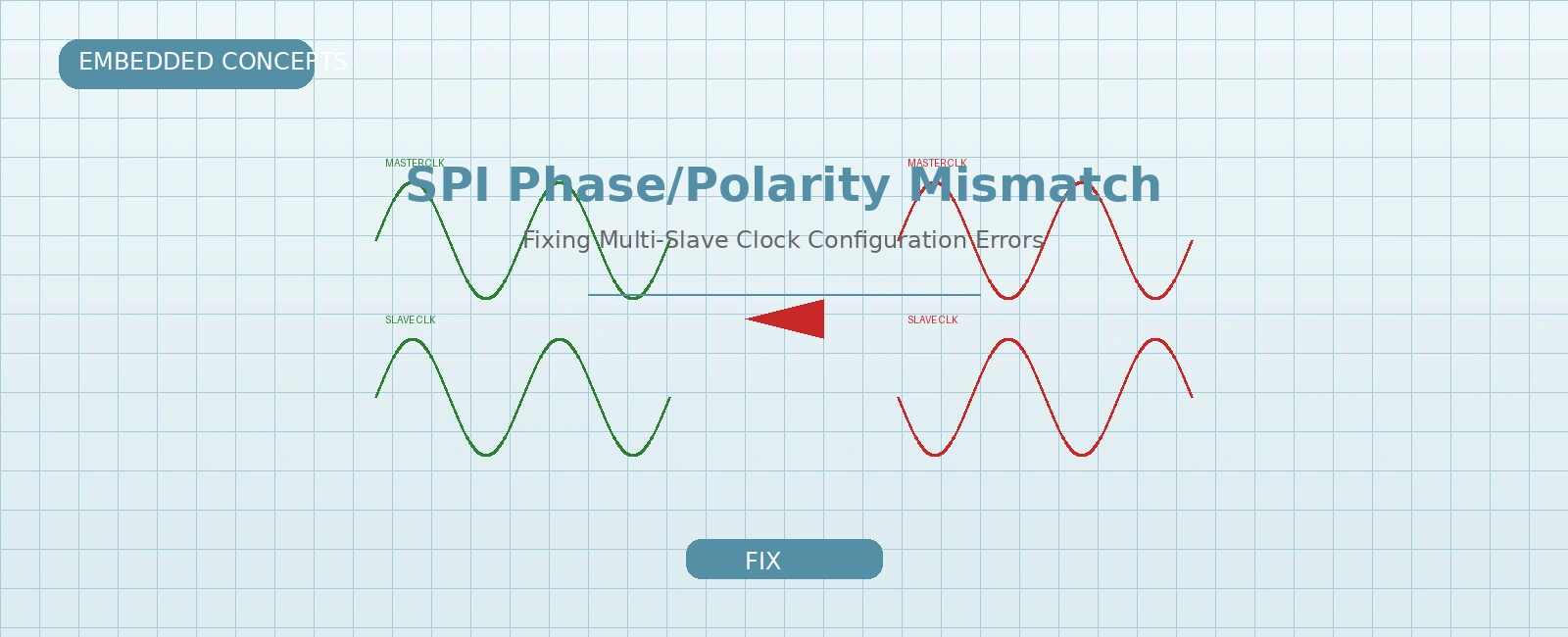
SPI clock phase and polarity mismatches are among the most deceptive failure modes in multi-slave embedded architectures. Firmware engineers frequently encounter this when expanding a functional bus: a microcontroller master communicates reliably with an SPI NOR flash, but adding an inertial sensor or precision ADC triggers sporadic data corruption, framing errors, or complete bus lockups.
In a common topology, the host controller shares SCK, MOSI, and MISO lines across an SPI flash requiring Mode 0 (CPOL=0, CPHA=0) and an environmental sensor requiring Mode 3 (CPOL=1, CPHA=1), driving distinct Chip Select (/CS) lines. If the master peripheral remains statically configured in Mode 0, it leaves SCK idling low. When /CS asserts for the Mode 3 sensor, the sensor observes SCK low instead of high, violating clock setup constraints. When clock pulses begin, the master samples MISO on the leading rising edge before the slave has shifted out its first data bit. The master reads invalid or shifted data, yet no peripheral overrun or bus fault interrupt is triggered.
In safety-critical nodes and telemetry units, subtle phase misalignments corrupt sensor readings without triggering hardware error flags, leading to invalid closed-loop decisions. In firmware upgrade paths, an unverified mode switch can corrupt flash verification pages. Resolving multi-slave SPI mode discrepancies requires an exact understanding of clock edge dynamics, per-transaction driver reconfiguration, and hardware controller capabilities.
The Serial Peripheral Interface (SPI) protocol, originally defined by Motorola, specifies four operating modes derived from two binary parameters: Clock Polarity (CPOL) and Clock Phase (CPHA).
// Standard Motorola SPI Mode Definitions// CPOL: Clock Polarity at idle state (0 = Low, 1 = High)// CPHA: Clock Phase / Sampling edge (0 = Leading/First Edge, 1 = Trailing/Second Edge)// Mode 0: CPOL=0, CPHA=0 -> Idle Low, Sample on Leading (Rising) Edge, Shift on Trailing (Falling) Edge// Mode 1: CPOL=0, CPHA=1 -> Idle Low, Shift on Leading (Rising) Edge, Sample on Trailing (Falling) Edge// Mode 2: CPOL=1, CPHA=0 -> Idle High, Sample on Leading (Falling) Edge, Shift on Trailing (Rising) Edge// Mode 3: CPOL=1, CPHA=1 -> Idle High, Shift on Leading (Falling) Edge, Sample on Trailing (Rising) Edge
Each slave peripheral has its SPI mode fixed in hardware. In single-slave topologies, the master peripheral is initialized once during boot. In multi-slave designs where peripherals require disparate modes, the master must handle dynamic mode switching.
When a master configured for Mode 0 communicates with a Mode 3 slave, three distinct electrical and protocol violations occur:
Idle State and Setup Timing Violation (t_CSS / t_LEAD):
Mode 3 devices require SCK to reside at logic high prior to and during chip select assertion. When the master leaves SCK low at /CS assertion, the slave’s internal state machine detects an illegal initial clock level. Some devices interpret the low level as an active clock state, causing an immediate bit-slip.
Half-Cycle Phase Shift and Stale Sampling: In Mode 0, the transmitter drives data before the first rising edge, and the receiver samples on that first edge. In Mode 3, data is shifted out on the falling edge and sampled on the rising edge. When the master clocks a Mode 3 slave with Mode 0 timing, the master samples MISO on the initial rising edge before the slave has executed its first shift transition. The master samples floating bus capacitance or stale output states, shifting all subsequently received bits by one position.
SCK Glitches during Dynamic CPOL Reconfiguration:
If firmware reconfigures CPOL while the SPI peripheral is actively enabled or while /CS is asserted, SCK transitions between logic low and high. This transition is seen by the slave as an illegitimate clock edge, inserting a rogue clock pulse into its internal shift register.
+------------------------------------------------------------------------------------+| SPI TIMING COMPARISON AND MODE MISMATCH FAILURE |+------------------------------------------------------------------------------------+--- MODE 0: CPOL=0, CPHA=0 (Idle Low, Sample on 1st/Leading Rising Edge) ---/CS : ----\___________________________________________________________/----SCK (Mode 0): _______/---\___/---\___/---\___/---\___/---\___/---\___/---\_________MOSI / MISO : ----| D7 | D6 | D5 | D4 | D3 | D2 | D1 | D0 |----Sample Edge : ^ ^ ^ ^ ^ ^ ^ ^(Data valid before rising edge; sampled on rising edge)--- MODE 3: CPOL=1, CPHA=1 (Idle High, Sample on 2nd/Trailing Rising Edge) ---/CS : ----\___________________________________________________________/----SCK (Mode 3): -------\___/---\___/---\___/---\___/---\___/---\___/---\___/---------MOSI / MISO : [Idle] | D7 | D6 | D5 | D4 | D3 | D2 | D1 | D0 |Sample Edge : ^ ^ ^ ^ ^ ^ ^ ^(Data shifted on falling edge; sampled on rising edge)--- MISMATCH: Master Configured in Mode 0 Clocks Mode 3 Slave ---/CS : ----\___________________________________________________________/----SCK (Master): _______/---\___/---\___/---\___/---\___/---\___/---\___/---\_________^ ^ (SCK starts LOW! Mode 3 slave expects HIGH idle on /CS assert)Master Rx : ^ ^ ^ ^ ^ ^ ^ ^Slave MISO : [Hi-Z/Stale] | D7 | D6 | D5 | D4 | D3 | D2 | D1 |Result Data : Master reads floating bus state on Edge 1 -> All bits shifted by 1 bit!+------------------------------------------------------------------------------------+
To prevent setup and hold violations during mixed-mode operation, all transactions must satisfy the following timing parameters:
t_CSS >= t_SU(CS) : /CS assertion setup time before first SCK transitiont_SU >= t_SU(DIN) : Serial data input setup time before sampling clock edget_HD >= t_HD(DIN) : Serial data input hold time after sampling clock edget_CSH >= t_HD(CS) : /CS hold time after final SCK transition before deassertiont_IDLE >= t_CS_HIGH_MIN : Deselect delay between consecutive /CS assertionsC_BUS = C_TRACE + sum(C_IN_i) <= C_MAX_SPEC (typically <= 50 pF)
In operating systems like Zephyr RTOS, peripheral drivers use dedicated device and configuration structures. The Zephyr SPI driver architecture cleanly binds bus attributes (frequency, operation flags, and chip select line) to a struct spi_config. When calling spi_transceive(), the core driver evaluates the operation field and dynamically reprograms the underlying hardware registers before asserting /CS.
#include <zephyr/kernel.h>#include <zephyr/drivers/spi.h>#include <zephyr/drivers/gpio.h>#include <zephyr/logging/log.h>LOG_MODULE_REGISTER(spi_mixed_modes, LOG_LEVEL_INF);/* Structure holding context for two slaves with different SPI modes */struct multi_slave_spi_bus {const struct device *bus_dev;struct spi_config cfg_flash; /* Slave 0: Mode 0 (CPOL=0, CPHA=0) */struct spi_config cfg_sensor; /* Slave 1: Mode 3 (CPOL=1, CPHA=1) */};/* Initialize configurations with distinct CPOL/CPHA and CS control */void init_spi_slave_configs(struct multi_slave_spi_bus *bus){/* Flash Device: Mode 0 (CPOL=0, CPHA=0) -> No CPOL/CPHA flags set */bus->cfg_flash.frequency = 20000000U; /* 20 MHz */bus->cfg_flash.operation = SPI_WORD_SET(8) | SPI_TRANSFER_MSB;bus->cfg_flash.slave = 0;bus->cfg_flash.cs.gpio = GPIO_DT_SPEC_GET(DT_NODELABEL(flash_cs_node), gpios);bus->cfg_flash.cs.delay = 2U; /* 2 us delay after CS assert before SCK *//* Sensor Device: Mode 3 (CPOL=1, CPHA=1) -> Both CPOL and CPHA set */bus->cfg_sensor.frequency = 4000000U; /* 4 MHz */bus->cfg_sensor.operation = SPI_WORD_SET(8) | SPI_TRANSFER_MSB |SPI_MODE_CPOL | SPI_MODE_CPHA;bus->cfg_sensor.slave = 1;bus->cfg_sensor.cs.gpio = GPIO_DT_SPEC_GET(DT_NODELABEL(sensor_cs_node), gpios);bus->cfg_sensor.cs.delay = 5U; /* 5 us delay for sensor internal wake/setup */}/* Transaction to Flash (Mode 0) */int read_flash_page(struct multi_slave_spi_bus *bus, uint32_t addr, uint8_t *rx_buf, size_t len){uint8_t cmd[4] = {0x03U,(uint8_t)((addr >> 16) & 0xFFU),(uint8_t)((addr >> 8) & 0xFFU),(uint8_t)(addr & 0xFFU)};struct spi_buf tx_bufs[2] = {{ .buf = cmd, .len = sizeof(cmd) },{ .buf = NULL, .len = len } /* Clock dummy bytes */};struct spi_buf rx_bufs[2] = {{ .buf = NULL, .len = sizeof(cmd) }, /* Discard response during cmd */{ .buf = rx_buf, .len = len }};struct spi_buf_set tx = { .buffers = tx_bufs, .count = 2 };struct spi_buf_set rx = { .buffers = rx_bufs, .count = 2 };return spi_transceive(bus->bus_dev, &bus->cfg_flash, &tx, &rx);}/* Transaction to Sensor (Mode 3) */int read_sensor_register(struct multi_slave_spi_bus *bus, uint8_t reg_addr, uint8_t *rx_data, size_t len){uint8_t cmd = reg_addr | 0x80U; /* Read command bit */struct spi_buf tx_bufs[2] = {{ .buf = &cmd, .len = 1 },{ .buf = NULL, .len = len } /* Clock dummy bytes */};struct spi_buf rx_bufs[2] = {{ .buf = NULL, .len = 1 }, /* Discard response during cmd */{ .buf = rx_data, .len = len }};struct spi_buf_set tx = { .buffers = tx_bufs, .count = 2 };struct spi_buf_set rx = { .buffers = rx_bufs, .count = 2 };/* Driver automatically reconfigures hardware registers to Mode 3 */return spi_transceive(bus->bus_dev, &bus->cfg_sensor, &tx, &rx);}
Microcontrollers differ significantly in how their SPI peripherals handle mixed-mode bus arbitration:
High-end microcontrollers support dedicated per-chip-select registers in hardware, eliminating software reconfiguration overhead:
SPI_CSR[0..3]): The SPI controller provides four independent Chip Select Registers (SPI_CSR0 to SPI_CSR3). Each register independently sets CPOL, NCPHA, transfer size, and baud rate. Writing the destination slave index into the Transmit Data Register (SPI_TDR.PCS) causes the controller to load the matching CSR settings automatically.TCR): The Transmit Command Register (LPSPI_TCR) contains PCS, CPOL, CPHA, and clock prescaler fields. A write to the transmit FIFO updates the target chip select and SPI mode on the fly with zero inter-frame pause./* Microchip SAM E70 Hardware Per-CS Register Initialization */void sam_e70_spi_hw_multislave_init(Spi *spi_base){/* Enable SPI and set to Master Mode */spi_base->SPI_MR = SPI_MR_MSTR | SPI_MR_MODFDIS | SPI_MR_PCS(0);/* Channel 0 (CS0 - Flash): Mode 0 (CPOL=0, NCPHA=1 in SAM naming), 20 MHz */spi_base->SPI_CSR[0] = SPI_CSR_NCPHA | SPI_CSR_BITS_8_BIT | SPI_CSR_SCBR(6);/* Channel 1 (CS1 - Sensor): Mode 3 (CPOL=1, NCPHA=0 in SAM naming), 5 MHz */spi_base->SPI_CSR[1] = SPI_CSR_CPOL | SPI_CSR_BITS_8_BIT | SPI_CSR_SCBR(24);}
Controllers like the STM32 family use a single set of control registers (SPI_CR1 on F4/F7/G4 or SPI_CFG2 on H7). Changing modes requires a strict sequence:
/* Safe runtime mode switch for STM32H7 (RM0433) */void stm32h7_spi_set_mode(SPI_TypeDef *spi, uint32_t cpol, uint32_t cpha){/* 1. Wait until TX/RX FIFOs are empty and transmission completes */while ((spi->SR & SPI_SR_TXC) == 0U) { /* Wait for TX complete */ }/* 2. Disable SPI peripheral (SPE bit in CR1 must be 0 to modify CFG2) */spi->CR1 &= ~SPI_CR1_SPE;/* 3. Wait for SPE bit to clear in peripheral clock domain */while ((spi->CR1 & SPI_CR1_SPE) != 0U) { /* Spin until disabled */ }/* 4. Modify CPOL and CPHA in CFG2 */uint32_t cfg2 = spi->CFG2;cfg2 &= ~(SPI_CFG2_CPOL | SPI_CFG2_CPHA);if (cpol) cfg2 |= SPI_CFG2_CPOL;if (cpha) cfg2 |= SPI_CFG2_CPHA;spi->CFG2 = cfg2;/* 5. Re-enable SPI peripheral */spi->CR1 |= SPI_CR1_SPE;}
[!WARNING] On STM32 microcontrollers, writing to
SPI_CFG2(orSPI_CR1on Cortex-M4) whileSPEis set violates hardware sequencing constraints and is ignored by silicon logic. Always disableSPEbefore updating CPOL/CPHA.
When pins must be assigned to arbitrary GPIOs or when hardware SPI cannot reconfigure cleanly, a deterministic software bit-bang routine provides universal compatibility across all four modes.
#include <stdint.h>#include <stdbool.h>typedef enum {SPI_MODE_0 = 0x00, /* CPOL=0, CPHA=0 */SPI_MODE_1 = 0x01, /* CPOL=0, CPHA=1 */SPI_MODE_2 = 0x02, /* CPOL=1, CPHA=0 */SPI_MODE_3 = 0x03 /* CPOL=1, CPHA=1 */} spi_mode_e;/* Microsecond-range delay tuned for target bus frequency */static inline void spi_delay_half_period(void){for (volatile int i = 0; i < 15; i++) { __asm__ volatile("nop"); }}/* Fully compliant 8-bit full-duplex SPI bit-bang transfer */uint8_t spi_bb_transfer(void (*set_sck)(bool), void (*set_mosi)(bool),bool (*get_miso)(void), spi_mode_e mode, uint8_t tx_byte){uint8_t rx_byte = 0;bool cpol = (mode & 0x02) != 0;bool cpha = (mode & 0x01) != 0;/* Ensure SCK begins in idle state */set_sck(cpol);spi_delay_half_period();for (int bit = 7; bit >= 0; bit--) {bool tx_bit = ((tx_byte >> bit) & 0x01) != 0;if (!cpha) {/* CPHA=0: Transmitter drives MOSI before leading clock edge */set_mosi(tx_bit);spi_delay_half_period();/* Leading edge: Receiver samples */set_sck(!cpol);spi_delay_half_period();rx_byte = (uint8_t)((rx_byte << 1) | (get_miso() ? 1 : 0));/* Trailing edge: Return clock to idle */set_sck(cpol);} else {/* CPHA=1: Leading edge is the shift edge */set_sck(!cpol);set_mosi(tx_bit);spi_delay_half_period();/* Trailing edge: Receiver samples */set_sck(cpol);spi_delay_half_period();rx_byte = (uint8_t)((rx_byte << 1) | (get_miso() ? 1 : 0));}}/* Final hold in idle state */set_sck(cpol);spi_delay_half_period();return rx_byte;}
When connecting four or more mixed-mode slaves, capacitive loading on shared clock and data traces degrades transition times. An analog/digital bus multiplexer (e.g., TI TS3A27518E, SN74CBTLV3257, or ADG734) isolates branches, keeps bus capacitance below 15 pF per leg, and prevents clock edge glitches from reaching deselected devices.
+--------------------------------------------------------------------------------+| SPI BUS MULTIPLEXING AND BUS ISOLATION ARCHITECTURE |+--------------------------------------------------------------------------------+| || +--------------------+ || | MCU HOST MASTER | || | (Dynamic Mode Re- |--- SCK / MOSI / MISO ----------------+ || | configuration) | | || | |--- MUX SEL [A, B] -------------------+ || | | | || | |--- /CS0, /CS1 -----------------------+ || +--------------------+ | || v || +----------------------------+ || | BUS SWITCH / MUX | || | (e.g., TI TS3A27518E) | || +----------------------------+ || | | || Branch 0 (Bank A) Branch 1 (Bank B) || Isolated Sub-bus Isolated Sub-bus || | | || v v || +-------------+ +-------------+|| | SLAVE 0 | | SLAVE 1 ||| | (Flash) | | (Sensor) ||| | Mode 0 | | Mode 3 ||| +-------------+ +-------------+|| |+--------------------------------------------------------------------------------+
[!NOTE] Passive multiplexers isolate physical traces and capacitance; they do not perform protocol conversion. The host MCU must still adjust CPOL and CPHA before selecting each respective multiplexer branch.
Compile a comprehensive table of all peripherals sharing the bus:
| Device | Part Number | Required Mode | Max SCK Frequency | t_SU (DIN Setup) | t_CSS (CS Setup) |
|---|---|---|---|---|---|
| Flash NOR | W25Q128JV | Mode 0 (or 3) | 133 MHz | 2.0 ns | 3.0 ns |
| IMU Sensor | BMI088 | Mode 3 (or 0) | 10 MHz | 5.0 ns | 20.0 ns |
| Precision ADC | ADS1256 | Mode 1 | 2 MHz | 50.0 ns | 50.0 ns |
When capturing multi-slave SPI signals:
10 * f_SCK (e.g., >= 100 MS/s for a 10 MHz bus)./CS0, /CS1, SCK, MOSI, and MISO concurrently./CS.>= 2 us prior to /CS falling edge to verify SCK idle polarity.To verify that the MCU peripheral driver switches phase and polarity without register lockup, implement an automated loopback test by externally jumpering MOSI to MISO:
int spi_mode_loopback_verify(const struct device *spi_dev, struct spi_config *cfg){static const uint8_t test_pattern[8] = {0x55U, 0xAAU, 0x00U, 0xFFU, 0x12U, 0x34U, 0x56U, 0x78U};uint8_t rx_buf[sizeof(test_pattern)] = {0};struct spi_buf tx_buf = { .buf = (void *)test_pattern, .len = sizeof(test_pattern) };struct spi_buf rx_buf_desc = { .buf = rx_buf, .len = sizeof(rx_buf) };struct spi_buf_set tx = { .buffers = &tx_buf, .count = 1 };struct spi_buf_set rx = { .buffers = &rx_buf_desc, .count = 1 };int ret = spi_transceive(spi_dev, cfg, &tx, &rx);if (ret != 0) {LOG_ERR("SPI transceive failed with status %d", ret);return ret;}for (size_t i = 0; i < sizeof(test_pattern); i++) {if (rx_buf[i] != test_pattern[i]) {LOG_ERR("Loopback mismatch at idx %zu: sent 0x%02X, received 0x%02X",i, test_pattern[i], rx_buf[i]);return -EIO;}}LOG_INF("Mode 0x%X loopback test passed", cfg->operation);return 0;}
>= 100000 consecutive alternating transactions (Slave 0 (Mode 0) <-> Slave 1 (Mode 3)). Verify zero bit-slips or framing faults.VDD +/- 10% to verify edge rate slew and logic thresholds (V_IH / V_IL).-40 deg C to +85 deg C to reveal setup/hold degradation caused by trace capacitance and driver temperature drift.| Test ID | Sequence | Mode Sequence | Target Peripherals | Acceptance Criteria |
|---|---|---|---|---|
| TC-01 | Single Device Baseline | Mode 0 | Flash NOR | 100% correct page reads |
| TC-02 | Single Device Baseline | Mode 3 | IMU Sensor | 100% valid WHO_AM_I register reads |
| TC-03 | Rapid Alternation | Mode 0 -> Mode 3 | Flash -> Sensor | 0 framing errors across 10k transfers |
| TC-04 | Rapid Alternation | Mode 3 -> Mode 0 | Sensor -> Flash | 0 framing errors across 10k transfers |
| TC-05 | Bus Idle Glitch Check | CS deasserted | Oscilloscope on SCK | No spurious voltage pulses > 0.3 * VDD |
SPI clock phase and polarity mismatches in multi-slave designs stem from mismatched hardware expectations between master and slave peripherals. Overcoming this requires disciplined software and hardware practices:
/CS assertion.t_IDLE) and clock lead times (t_CSS) so that the slave recognizes the clock idle level before sampling begins.Quick Links
Legal Stuff