

Bitwise Modulo in C: Optimizing Embedded Systems
September 26, 2026
5 min
UART receiver overrun errors are among the most persistent failure modes in embedded real-time systems operating at high baud rates. On NXP i.MX RT crossover microcontrollers (powered by Arm Cortex-M7 cores running up to 600 MHz or 1 GHz), high core clock speeds can create a false sense of security regarding serial communication responsiveness.
Standard serial communication on the i.MX RT platform is handled by the Low-Power UART (LPUART) peripheral. In interrupt-driven architectures, each received character or FIFO watermark threshold triggers a peripheral interrupt request (IRQ) to the Nested Vectored Interrupt Controller (NVIC). If higher-priority interrupts (such as motor control FOC loops, USB, or Ethernet ISRs) or critical sections protected by interrupt-disabling primitives (__disable_irq()) preempt or block the UART ISR longer than the time required to fill the remaining hardware FIFO slots, incoming data overwrites unserviced buffer space.
When an overrun occurs:
STAT[OR] in LPUART, or SHIFTERR in FlexIO).In sensor telemetry, industrial fieldbuses, and high-throughput communication protocols, overrun errors produce silent payload truncations, frame checksum failures, and protocol state machine desynchronization.
The fundamental cause of a UART overrun error is a timing mismatch between wire-speed byte arrival and the system’s servicing latency. Key contributing factors include:
WATER[RXWATER]) is misconfigured, the interrupt triggers too late to provide sufficient latency headroom.Consider standard 8N1 asynchronous serial framing (1 start bit, 8 data bits, no parity bit, 1 stop bit = 10 bits per character frame). The timing equations governing bit duration, character duration, and FIFO fill time are defined as follows:
Baud Rate (B) = 921,600 bits/secondBit Duration (T_bit) = 1 / B = 1 / 921,600 s = 1.08507 us (1085.07 ns)Framing (8N1): 1 Start bit + 8 Data bits + 0 Parity bits + 1 Stop bit = 10 bits/frameCharacter Duration (T_frame) = 10 * T_bit = 10.8507 usHardware FIFO Depth (N_fifo) = 4 bytes (PARAM[RXFIFO] = 4)Total Buffer Fill Duration (T_fill) = N_fifo * T_frame = 4 * 10.8507 us = 43.4028 us
If the receive watermark is set to zero (WATER[RXWATER] = 0), the first byte placed into an empty FIFO immediately sets the Receive Data Register Full flag (STAT[RDRF]) and generates an interrupt. The CPU has a window of exactly 3 incoming frames plus the stop-bit interval before the 5th frame overflows the FIFO:
Max Allowable Interrupt Latency = 3 * T_frame + T_frame = 43.4028 us
However, if WATER[RXWATER] is set to 3 (triggering when 4 bytes are present), the interrupt is not asserted until the 4th byte is fully received. The CPU has only a single byte frame duration to respond:
Allowable Interrupt Latency Margin = 1 * T_frame = 10.8507 us
At 3,000,000 baud (3 MBaud), this margin collapses catastrophically:
B = 3,000,000 bits/secondT_bit = 1 / 3,000,000 s = 333.33 nsT_frame = 10 * 333.33 ns = 3.333 us4-Byte FIFO Saturation Duration = 4 * 3.333 us = 13.333 usLatency Margin (RXWATER = 3) = 3.333 us
Any ISR or flash wait state delay exceeding 3.33 us triggers a guaranteed hardware overrun.
+-----------------------------------------------------------------------------+| UART OVERRUN TIMING ANALYSIS (921600 BAUD) |+-----------------------------------------------------------------------------+| Baud: 921600 (T_bit = 1.085 us) | Frame: 8N1 (10 bits = 10.85 us per byte) || Hardware FIFO: 4 bytes (PARAM[RXFIFO] = 4) | Fill Time: 43.4 us || || Time ---> 0 us 10.85 us 21.70 us 32.55 us 43.40 us|| | | | | | || RX Pin +-[Start..Stop]+-[Start..Stop]+-[Start..Stop]+-[Start..Stop]+ ... || Bytes | Byte 0 | Byte 1 | Byte 2 | Byte 3 |Byte 4|| +--------------+--------------+--------------+-------------+------+| || Hardware +--------------+--------------+--------------+-------------+ || RX FIFO | Slot 0: B0 | Slot 1: B1 | Slot 2: B2 | Slot 3: B3 | FULL!|| (4 bytes) +--------------+--------------+--------------+-------------+ || ^ | || | Watermark RXWATER = 0 triggers IRQ | || v || CPU ISR [------ High-Priority Task / ISR Delay: > 43.4 us -------] OVERRUN|| Latency STAT[OR|| assert || Byte 4 || DROPPED|+-----------------------------------------------------------------------------+| OFFLOADING WITH eDMA / FlexIO |+-----------------------------------------------------------------------------+| || RX Pin +-- Byte 0 --+-- Byte 1 --+-- Byte 2 --+-- Byte 3 --+-- Byte 4 --+|| +------------+------------+------------+------------+------------+|| | | | | | || Trigger v (eDMA req) v (eDMA req) v (eDMA req) v (eDMA req) v (eDMA)|| eDMA +----------------------------------------------------------------+|| Engine | Transfers each byte to SRAM in ~20 ns bus cycles (Zero CPU Load)|| +----------------------------------------------------------------+|| | | | | | || SRAM +-----+------+-----+------+-----+------+-----+------+-----+------+|| Ring Buf | Slot 0: B0 | Slot 1: B1 | Slot 2: B2 | Slot 3: B3 | Slot 4: B4 | ...| (256 B) +------------+------------+------------+------------+------------+|| || Result: Zero Overrun Errors; Hardware Latency << 10.85 us byte period |+-----------------------------------------------------------------------------+
To maximize CPU response headroom without altering hardware architecture:
WATER[RXWATER] = 0 so that STAT[RDRF] fires on the first received character.LPUARTx->DATA and writing into a lock-free circular ring buffer. Avoid parsing or logging within ISR context.The Enhanced Direct Memory Access (eDMA) controller on i.MX RT routes hardware DMA requests from LPUART (kDmaRequestMuxLPUART1Rx) directly to eDMA channels. Each received character triggers a single-byte minor loop transfer from LPUARTx->DATA to SRAM. The transfer completes in tens of nanoseconds on the internal AXI/AHB bus crossbar, eliminating the CPU interrupt latency bottleneck entirely.
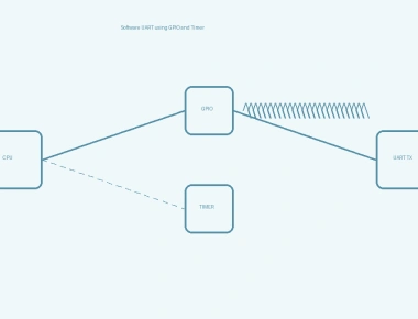
When all dedicated LPUART peripherals are allocated, or when pin routing conflicts with high-speed memory interfaces (e.g., SEMC SDRAM or FlexSPI NOR Flash), NXP’s FlexIO (Flexible Input/Output) module provides a programmable hardware state machine.
FlexIO consists of:
SHIFTBUF[n]).TIMCMP[n]) operating up to 120 MHz.FXIO_D0 through FXIO_D31).FlexIO shifts serial UART bits into SHIFTBUF[n] and raises a DMA request (kDmaRequestMuxFlexIO1Request0) upon word reception. By pairing FlexIO with eDMA, developers gain dedicated, jitter-immune UART channels that run reliably at multi-megabaud rates without CPU intervention.
+-----------------------------------------------------------------------------+| FLEXIO UART RX TO eDMA PIPELINE |+-----------------------------------------------------------------------------+| || RX Pin (FXIO_D1) || | || +----------> [FlexIO Timer 1] || | - Dual 8-bit baud counter (Baud clock generator) || | - Triggered on falling edge (Start bit detection) || | - Generates shift pulses on bit centers || | | || | v (Shift clock) || +----------> [FlexIO Shifter 1] || - Configured in SMR receive mode || - Shifts 8 bits serially from pin FXIO_D1 || - Latches complete character into SHIFTBUF[1] || | || v (Shifter Status Flag: SHIFTSTAT[1] = 1) || [DMAMUX Request: kDmaRequestMuxFlexIO1Request0] || | || v (Hardware DMA Trigger) || [eDMA Channel Transfer Control Descriptor (TCD)] || - Source: &FLEXIO1->SHIFTBUF[1] || - Destination: SRAM Circular Buffer (Non-cacheable) || - Clears SHIFTSTAT[1] automatically on read || |+-----------------------------------------------------------------------------+
A critical requirement on the i.MX RT platform is memory coherency. The Cortex-M7 core features a 32 KB L1 Data Cache (D-Cache). Because eDMA writes data directly to physical SRAM over the system bus, the D-Cache does not automatically snoop peripheral bus transactions.
To avoid data corruption or stale reads:
SCB_InvalidateDCache_by_Addr().SDK_ALIGN(buf, 32)) and sized to a multiple of 32 bytes. This prevents false sharing, where invalidating a cache line inadvertently corrupts adjacent variables.This example configures LPUART1 on i.MX RT using the MCUXpresso SDK. Incoming data is transferred directly into an SRAM ring buffer via eDMA channel 0. The LPUART Idle-Line interrupt detects frame completions without byte-by-byte CPU overhead.
#include "fsl_common.h"#include "fsl_lpuart.h"#include "fsl_edma.h"#include "fsl_dmamux.h"#include "fsl_clock.h"#define LPUART_BASE LPUART1#define LPUART_CLK_FREQ CLOCK_GetFreq(kCLOCK_UartClk)#define LPUART_DMA_MUX_SRC kDmaRequestMuxLPUART1Rx#define LPUART_EDMA_CHANNEL 0U#define RX_BUFFER_SIZE 256U/* Align buffer to 32-byte Cortex-M7 D-Cache line boundary */SDK_ALIGN(static uint8_t s_rxBuffer[RX_BUFFER_SIZE], 32);static edma_handle_t s_edmaHandle;static volatile uint32_t s_rxReadIndex = 0U;void LPUART1_IRQHandler(void){uint32_t status = LPUART_GetStatusFlags(LPUART_BASE);/* Check and clear Overrun Error Flag */if ((status & kLPUART_RxOverrunFlag) != 0U){LPUART_ClearStatusFlags(LPUART_BASE, kLPUART_RxOverrunFlag);}/* Check for IDLE line detection (end of burst frame) */if ((status & kLPUART_IdleLineFlag) != 0U){LPUART_ClearStatusFlags(LPUART_BASE, kLPUART_IdleLineFlag);/* Determine current write position from remaining major loop count */uint32_t remainingBytes = EDMA_GetRemainingMajorLoopCount(DMA0, LPUART_EDMA_CHANNEL);uint32_t currentWriteIndex = RX_BUFFER_SIZE - remainingBytes;/* Invalidate D-Cache to ensure CPU reads updated SRAM data */SCB_InvalidateDCache_by_Addr((uint32_t *)s_rxBuffer, RX_BUFFER_SIZE);while (s_rxReadIndex != currentWriteIndex){uint8_t receivedByte = s_rxBuffer[s_rxReadIndex];s_rxReadIndex = (s_rxReadIndex + 1U) % RX_BUFFER_SIZE;(void)receivedByte; /* Forward to application queue or parser */}}SDK_ISR_EXIT_BARRIER;}void init_lpuart_edma(void){lpuart_config_t uartConfig;edma_config_t edmaConfig;edma_transfer_config_t transferConfig;/* 1. Initialize DMAMUX and route LPUART1 RX to eDMA Channel 0 */DMAMUX_Init(DMAMUX0);DMAMUX_SetSource(DMAMUX0, LPUART_EDMA_CHANNEL, LPUART_DMA_MUX_SRC);DMAMUX_EnableChannel(DMAMUX0, LPUART_EDMA_CHANNEL);/* 2. Initialize eDMA engine */EDMA_GetDefaultConfig(&edmaConfig);EDMA_Init(DMA0, &edmaConfig);EDMA_CreateHandle(&s_edmaHandle, DMA0, LPUART_EDMA_CHANNEL);/* 3. Configure circular transfer control descriptor (TCD) */EDMA_PrepareTransfer(&transferConfig,(void *)&LPUART_BASE->DATA,sizeof(uint8_t),(void *)s_rxBuffer,sizeof(uint8_t),sizeof(uint8_t),RX_BUFFER_SIZE,kEDMA_PeripheralToMemory);EDMA_SubmitTransfer(&s_edmaHandle, &transferConfig);/* Configure circular destination address reload upon major loop complete */DMA0->TCD[LPUART_EDMA_CHANNEL].DOFF = 1;DMA0->TCD[LPUART_EDMA_CHANNEL].DLAST_SGA = -(int32_t)RX_BUFFER_SIZE;EDMA_EnableAutoStopRequest(DMA0, LPUART_EDMA_CHANNEL, false);/* 4. Configure LPUART1 */LPUART_GetDefaultConfig(&uartConfig);uartConfig.baudRate_Bps = 921600U;uartConfig.enableTx = true;uartConfig.enableRx = true;uartConfig.rxFifoWatermark = 0U; /* Trigger DMA on first available byte */LPUART_Init(LPUART_BASE, &uartConfig, LPUART_CLK_FREQ);/* Enable RX DMA request and Idle-Line Interrupt */LPUART_EnableRxDMA(LPUART_BASE, true);LPUART_EnableInterrupts(LPUART_BASE, kLPUART_IdleLineInterruptEnable);EnableIRQ(LPUART1_IRQn);/* Start eDMA channel reception */EDMA_StartTransfer(&s_edmaHandle);}
This example configures the FlexIO module as an emulated UART receiver operating with eDMA. Incoming bytes on pin FXIO_D1 are transferred directly to SRAM without CPU intervention.
#include "fsl_common.h"#include "fsl_flexio_uart.h"#include "fsl_edma.h"#include "fsl_dmamux.h"#include "fsl_clock.h"#define BOARD_FLEXIO_BASE FLEXIO1#define FLEXIO_UART_TX_PIN 0U /* FXIO_D0 */#define FLEXIO_UART_RX_PIN 1U /* FXIO_D1 */#define FLEXIO_EDMA_CHANNEL 1U#define FLEXIO_DMA_MUX_SRC kDmaRequestMuxFlexIO1Request0#define RX_BUFFER_SIZE 256USDK_ALIGN(static uint8_t s_flexioRxBuffer[RX_BUFFER_SIZE], 32);static FLEXIO_UART_Type s_flexioUartDev;static edma_handle_t s_flexioEdmaHandle;void init_flexio_uart_edma(void){flexio_uart_config_t uartConfig;edma_config_t edmaConfig;edma_transfer_config_t transferConfig;/* 1. Map hardware pins, shifters, and timers to the FlexIO UART instance */s_flexioUartDev.flexioBase = BOARD_FLEXIO_BASE;s_flexioUartDev.TxPinIndex = FLEXIO_UART_TX_PIN;s_flexioUartDev.RxPinIndex = FLEXIO_UART_RX_PIN;s_flexioUartDev.shifterIndex[0] = 0U; /* TX shifter */s_flexioUartDev.shifterIndex[1] = 1U; /* RX shifter */s_flexioUartDev.timerIndex[0] = 0U; /* TX timer */s_flexioUartDev.timerIndex[1] = 1U; /* RX timer *//* 2. Configure FlexIO UART parameters */FLEXIO_UART_GetDefaultConfig(&uartConfig);uartConfig.baudRate_Bps = 921600U;uartConfig.enableTx = true;uartConfig.enableRx = true;FLEXIO_UART_Init(&s_flexioUartDev, &uartConfig, CLOCK_GetFreq(kCLOCK_Flexio1Clk));/* 3. Configure DMAMUX and eDMA Channel 1 */DMAMUX_Init(DMAMUX0);DMAMUX_SetSource(DMAMUX0, FLEXIO_EDMA_CHANNEL, FLEXIO_DMA_MUX_SRC);DMAMUX_EnableChannel(DMAMUX0, FLEXIO_EDMA_CHANNEL);EDMA_GetDefaultConfig(&edmaConfig);EDMA_Init(DMA0, &edmaConfig);EDMA_CreateHandle(&s_flexioEdmaHandle, DMA0, FLEXIO_EDMA_CHANNEL);/* 4. Set up eDMA transfer directly from FlexIO RX buffer address */uint32_t rxBufferAddr = FLEXIO_UART_GetRxBufferAddress(&s_flexioUartDev);EDMA_PrepareTransfer(&transferConfig,(void *)rxBufferAddr,sizeof(uint8_t),(void *)s_flexioRxBuffer,sizeof(uint8_t),sizeof(uint8_t),RX_BUFFER_SIZE,kEDMA_PeripheralToMemory);EDMA_SubmitTransfer(&s_flexioEdmaHandle, &transferConfig);/* Enable continuous auto-reload for circular streaming */DMA0->TCD[FLEXIO_EDMA_CHANNEL].DOFF = 1;DMA0->TCD[FLEXIO_EDMA_CHANNEL].DLAST_SGA = -(int32_t)RX_BUFFER_SIZE;EDMA_EnableAutoStopRequest(DMA0, FLEXIO_EDMA_CHANNEL, false);/* 5. Enable FlexIO RX DMA request and start transfer */FLEXIO_UART_EnableRxDMA(&s_flexioUartDev, true);EDMA_StartTransfer(&s_flexioEdmaHandle);}bool check_flexio_overrun(void){/* In FlexIO, overrun asserts the Shifter Error flag */uint32_t errorFlags = FLEXIO_GetShifterErrorFlags(BOARD_FLEXIO_BASE);uint32_t rxShifterMask = (1U << s_flexioUartDev.shifterIndex[1]);if ((errorFlags & rxShifterMask) != 0U){/* Clear error flag by writing 1 to the corresponding bit */FLEXIO_ClearShifterErrorFlags(BOARD_FLEXIO_BASE, rxShifterMask);return true;}return false;}
To rigorously verify that UART overrun errors are fully resolved:
LPUARTx->STAT. Bit 19 is the OR (Receiver Overrun) flag. Ensure STAT[OR] == 0 during continuous throughput testing.FLEXIOx->SHIFTERR. Ensure the bit corresponding to the RX shifter index remains zero.GPIO1_IO02) to toggle high immediately if an overrun flag is detected in firmware. Connect a logic analyzer with channel 0 on UART RX and channel 1 on the debug GPIO. Trigger on the rising edge of the debug pin to capture the exact bus traffic preceding an overrun.0x00 through 0xFF) at maximum baud rate using a hardware signal generator or USB-to-UART bridge (e.g., FT232H). Run transfers across 100 million characters and verify zero frame errors, zero overrun assertions, and complete checksum matching.UART overrun errors on NXP i.MX RT microcontrollers stem from the mismatch between microsecond byte arrival times and interrupt handling latencies. While adjusting LPUART FIFO watermarks (WATER[RXWATER] = 0) improves CPU response headroom, real-time deterministic communication at high baud rates requires hardware offloading.
By coupling LPUART or FlexIO with the eDMA controller, data bytes are transferred directly into SRAM circular buffers within nanoseconds of arrival. This completely decouples serial reception from CPU load, neutralizes interrupt latency bottlenecks, and guarantees zero-loss serial communication across mission-critical embedded systems.
Quick Links
Legal Stuff