

Embedded Linux: Fixing Slow Boot Time
August 30, 2026
8 min
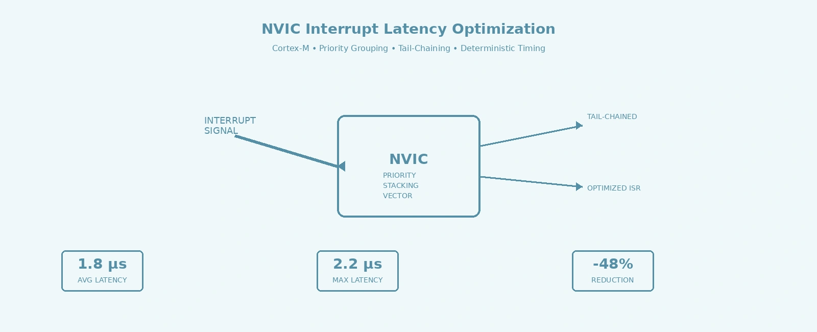
Interrupt latency is the cornerstone metric governing determinism in real-time embedded systems. In hard real-time domains—such as motor field-oriented control (FOC), high-speed industrial Ethernet transceivers, medical respirators, and switch-mode power topologies—a delayed or jittery interrupt response degrades control loop phase margins and can trigger catastrophic hardware faults.
In the ARM Cortex-M processor family (Armv7-M, Armv8-M, and Armv6-M), the Nested Vectored Interrupt Controller (NVIC) is integrated directly into the processor core rather than situated as an external peripheral on the system bus. While this tight coupling provides industry-leading responsiveness, developers often observe significant jitter and unexpected delays in production firmware. These delays stem from multi-cycle instruction retirement, flash memory wait states, floating-point register stacking penalties, store-buffer drain latencies, and misconfigured priority grouping schemes.
This guide analyzes the cycle-accurate mechanics of Cortex-M exception entry, debunks common architectural misconceptions regarding interrupt controller timing, and presents production-grade C techniques to achieve minimal, deterministic latency.
+---------------------------------------------------------------------------------------+| CORTEX-M EXCEPTION ENTRY PIPELINE FLOW |+---------------------------------------------------------------------------------------+Peripheral / External Event|v[ Interrupt Request Asserted ]|v[ Clock Synchronization Stage ] -------------> 1 to 3 Core Clock Cycles|v[ Priority Arbitration & Masking ] ----------> Evaluated combinationally against BASEPRI|v[ Instruction Boundary Resolution ] ---------> Completes current instruction or abandons| interruptible multi-cycle load/store+-----------------------+| |v v(Data Bus: AHB/AXI) (Code Bus: I-Code)+-------------------------+ +-------------------------+| Context Stacking | | Vector Address Fetch || Pushes R0-R3, R12, LR, | | Reads 32-bit vector || PC, xPSR to SP_main/ | | entry from VTOR + offset| SP_process (12 cycles)| | in parallel with stack |+-------------------------+ +-------------------------+| |+-----------+-----------+|v[ Pipeline Fetch & Decode ]|v[ First Instruction of ISR Executes ]
Figure 1: Cycle-accurate exception entry flow in ARM Cortex-M3/M4/M7 cores, highlighting concurrent dual-bus operations.
In legacy microcontrollers (such as ARM7TDMI or classic 8051/PIC devices), interrupt handling required software dispatch routines that saved registers via assembly instructions, read peripheral interrupt vectors, and branched to handler addresses. The ARM Cortex-M NVIC automates this sequence entirely in hardware.
External interrupt signals routed through chip-level GPIO pins or peripheral logic must pass through dual flip-flop synchronizers to prevent metastability across asynchronous clock boundaries. This adds 1 to 3 core processor clock cycles before the NVIC peripheral logic registers the interrupt as pending.
ARM Cortex-M processors take interrupts on instruction boundaries. If a single-cycle instruction (such as ADD, MOV, or AND) is currently in the execute stage of the pipeline, it completes in that cycle.
However, if a multi-cycle instruction is executing, standard Cortex-M implementations behave as follows:
LDM, STM, PUSH, POP): On Cortex-M3, Cortex-M4, and Cortex-M7 cores, multi-cycle load and store operations are interruptible and abandonable. The core abandons the multi-cycle instruction mid-stream without updating register state, services the interrupt immediately, and restarts the instruction upon return (PC points to the abandoned instruction). Alternatively, on cores utilizing the Interrupt-Continuable Instruction (ICI) bits in the xPSR, execution resumes from the interrupted register transfer.UDIV, SDIV): Division takes between 2 and 12 cycles depending on operand magnitude. On Cortex-M3/M4, division operations can be abandoned immediately upon interrupt arrival.The hallmark of Cortex-M exception entry is hardware context stacking performed concurrently with vector fetching:
MSP or PSP): R0, R1, R2, R3, R12, LR (R14), PC (R15), and xPSR.VTOR + (IRQn + 16) * 4 onto the code bus (I-Code or Flash interface) to retrieve the 32-bit starting address of the target ISR.Because the Cortex-M Harvard architecture features independent Code (I-Code) and System/Data (D-Code / System AHB) buses, the vector fetch overlaps with register stacking.
On Cortex-M3, Cortex-M4, and Cortex-M33 cores operating with zero-wait-state memory, this hardware sequence completes in exactly 12 clock cycles.
+-----------------------------------------------------------------------------------------+| CORE LATENCY & TAIL-CHAINING COMPARISON TABLE |+-------------------+--------------------+------------------------+-----------------------+| Processor Core | Baseline Entry | Tail-Chaining Latency | Hardware Architecture || | (Zero Wait States) | (Zero Wait States) | Pipeline Features |+-------------------+--------------------+------------------------+-----------------------+| Cortex-M0 | 16 cycles | N/A (not supported) | 2-stage von Neumann || Cortex-M0+ | 15 cycles | 13 cycles | 2-stage von Neumann || Cortex-M3 | 12 cycles | 6 cycles | 3-stage Harvard || Cortex-M4 / M4F | 12 cycles | 6 cycles | 3-stage Harvard + DSP || Cortex-M7 | 12 cycles (TCM) | 6 cycles (TCM) | 6-stage dual-issue || Cortex-M23 | 15 cycles | 13 cycles | 2-stage TrustZone || Cortex-M33 | 12 cycles (NS->NS) | 6 cycles | 3-stage TrustZone |+-------------------+--------------------+------------------------+-----------------------+
[!NOTE] The Cortex-M0 (Armv6-M) does not implement tail-chaining. Each ISR exit performs a full unstack, and each new ISR entry performs a full stack push, even when back-to-back interrupts are pending.
To calculate worst-case interrupt latency (WCIL) for safety-critical systems, system architects must account for hardware synchronization, bus stalls, memory wait states, and software prologues.
On Cortex-M3/M4/M7/M33 cores with independent Code and Data buses, stacking and vector fetching execute concurrently. The hardware entry cost is therefore the longer of the two operations, not their sum:
T_latency = T_sync + max(T_insn, T_crit) + max(T_stack, T_vector) + T_prologueWhere:T_sync = Hardware clock synchronization delay (1 to 3 core cycles)T_insn = Maximum non-abandonable instruction stall or bus wait stateT_crit = Longest atomic critical section duration (PRIMASK or BASEPRI)T_stack = Context stacking duration across data bus (12 cycles at zero WS)T_vector = Vector fetch duration across code bus (overlapped with T_stack)T_prologue = Software execution time of compiler-generated stack frame (R4-R11)
On von Neumann bus cores (Cortex-M0, M0+, M23), stacking and vector fetching share a single bus and execute sequentially. On these cores, use T_stack + T_vector instead of max(T_stack, T_vector).
When the stack pointer references memory that requires bus wait states (e.g., external SRAM, PSRAM, or contested internal multi-master SRAM), stacking stalls the processor pipeline:
Cycles_stack = 12 + (8 * W_RAM)Where:12 = Baseline entry cost at zero wait states (includes 8 register pushesplus pipeline sequencing and bus arbitration overhead)8 = Number of additional wait-state penalties (one per 32-bit register:R0-R3, R12, LR, PC, xPSR)W_RAM = Data memory write wait states per 32-bit transfer
If the Vector Table Offset Register (SCB->VTOR) points to Flash memory operating with wait states, the vector read stalls completion of the exception sequence:
Cycles_vector = 2 + W_FlashWhere:2 = Baseline internal bus transfer cycles for I-Code transactionW_Flash = Flash read wait states (e.g., 5 wait states on STM32F4 at 168 MHz)
If W_Flash > 0 and the instruction bus is slower than the data bus stack push, vector retrieval becomes the critical path, extending entry latency beyond 12 cycles.
The Cortex-M NVIC implements three dedicated hardware mechanisms designed to eliminate redundant stacking operations when handling bursts of interrupts.
CASE A: Standard Sequential Interrupt Handling (No Tail-Chaining)+---------------+---------------+---------------+---------------+---------------+| ISR A Executes| Full Unstack | Idle/Thread | Full Stacking | ISR B Executes|| | (10-12 cycles)| (1+ cycles) | (12 cycles) | |+---------------+---------------+---------------+---------------+---------------+Total Inter-ISR Transition: ~22 to 25 Clock CyclesCASE B: NVIC Tail-Chaining Active+---------------+---------------+---------------+| ISR A Executes| Tail-Chain | ISR B Executes|| | (6 cycles) | |+---------------+---------------+---------------+Total Inter-ISR Transition: EXACTLY 6 Clock Cycles (68% to 76% Latency Reduction)
Figure 2: Execution timeline comparing conventional unstack/restack transitions against NVIC hardware tail-chaining.
When an ISR finishes execution and another interrupt is pending with eligible priority, returning to the interrupted background thread only to immediately re-enter an exception would waste over 20 clock cycles (unstacking 8 registers, executing BX LR, and immediately restacking 8 registers).
Instead, the NVIC intercepts the BX LR (EXC_RETURN) sequence:
R0-R3, R12, LR, PC, and xPSR.If Interrupt A (low priority) asserts first, the NVIC begins the 12-cycle context stacking sequence. If Interrupt B (high priority) asserts on cycle 7 of this stacking phase:
When Interrupt B finishes, Interrupt A is serviced via tail-chaining in 6 cycles. This prevents high-priority interrupts from being blocked by lower-priority context saves.
If a higher-priority interrupt arrives while the processor is in the middle of unstacking registers (popping context) at the conclusion of an ISR, the NVIC halts the pop sequence, preserves the remaining stack frame, and switches directly to servicing the new interrupt.
A persistent myth in embedded software engineering claims that certain PRIGROUP configurations in SCB->AIRCR take “extra clock cycles to evaluate” due to asymmetric bitfield decoding in hardware.
[!IMPORTANT] Hardware Fact: The NVIC priority arbitration circuit is a fully parallel, fixed-width combinational comparator implemented in silicon gates. Regardless of whether
PRIGROUPis set to 0, 3, 5, or 7, priority comparison completes in the exact same fraction of a clock cycle. It introduces zero additional comparison cycles.
The real latency danger of PRIGROUP is logical rather than electrical. The 8-bit priority register (of which typical silicon vendors implement the top 3, 4, or 5 bits) is split into two fields:
+---------------------------------------------------------------------------------------+| 4-BIT NVIC PRIORITY REGISTER SPLIT (STM32 EXAMPLE) |+---------------------------------------------------------------------------------------+| Bit 7 | Bit 6 | Bit 5 | Bit 4 | Bit 3 (0) | Bit 2 (0) | Bit 1 (0) | Bit 0 (0) |+-------+-------+-------+-------+-----------+-----------+-----------+-------------------+|<-------- Preemption --------->| (Unimplemented / Read as Zero in 4-bit MCU) || (PRIGROUP = 3: 16 Preemption Levels, 0 Subpriority Levels - RECOMMENDED) |+-------------------------------+-------------------------------------------------------+|<-- Preempt -->|<-- Subprio -->| || (PRIGROUP = 5: 4 Preemption Levels, 4 Subpriority Levels) |+---------------+---------------+-------------------------------------------------------+
Consider two interrupts:
IRQ_MotorCurrent: Time-critical ADC sampling (budget: < 2 us).IRQ_UART_Rx: Low-priority byte reception (takes 15 us to read FIFO).If both IRQs are assigned Preemption Priority 2 with differing Subpriorities:
IRQ_UART_Rx is executing, IRQ_MotorCurrent asserts.IRQ_MotorCurrent cannot preempt IRQ_UART_Rx.IRQ_MotorCurrent experiences head-of-line blocking jitter equal to the entire 15 us runtime of the UART handler, causing an overrun.For deterministic real-time systems and RTOS kernels (such as FreeRTOS, Zephyr, and ThreadX), assign all implemented priority bits to preemption priority (PRIGROUP = 3 on 4-bit priority architectures like STM32):
/* Configure all 4 priority bits for preemption (0 subpriority bits) */NVIC_SetPriorityGrouping(3); /* CMSIS: NVIC_PriorityGroup_4 */
FPCCR.LSPEN) OptimizationOn Cortex-M4F, Cortex-M7, and Cortex-M33 devices equipped with a single-precision or double-precision Floating Point Unit, interrupt stacking behavior changes dramatically.
R0-R3, R12, LR, PC, xPSR) = 32 bytes (12 cycles).S0-S15) + FPSCR + 1 alignment word = 26 registers (104 bytes).Writing 104 bytes over a 32-bit bus requires at least 26 bus cycles. If an ISR must push the full FPU context, entry latency spikes from 12 cycles to over 27 cycles, introducing massive timing jitter into non-floating-point interrupts.
+---------------------------------------------------------------------------------------+| FPU LAZY STACKING HARDWARE MECHANICS |+---------------------------------------------------------------------------------------+Interrupt Asserts (Core in Thread Mode with FPU active)|v[ Check FPCCR.LSPEN Bit ]|+--------+--------+| |[LSPEN = 0] [LSPEN = 1] (Default CMSIS)| || +--> 1. Decrements SP by 104 bytes (reserving space)| 2. Writes ONLY integer registers R0-R3, R12, LR, PC, xPSR| 3. Sets FPCCR.LSPACT = 1 (Hardware Flag)| 4. Enters ISR in EXACTLY 12 CYCLES!| |v vEager Stacking: Does ISR execute any FPU instruction?Pushes all 26 registers |S0-S15 + FPSCR immediately +-------+-------+Takes 27+ clock cycles! | |(Severe Latency Jitter) [ NO ] [ YES ]| || +--> Hardware pauses pipeline,| dumps S0-S15 to reserved slot,| clears LSPACT, executes float.vReturns via EXC_RETURN:No FP registers ever written!Saved 15+ cycles on entry and exit!
In production firmware, verify that both Automatic Stacking (ASPEN) and Lazy Stacking (LSPEN) are enabled in the Floating Point Context Control Register (FPCCR):
void System_EnableFpuLazyStacking(void) {/* Enable lazy stacking: reserve space without writing S0-S15 */FPU->FPCCR |= (FPU_FPCCR_ASPEN_Msk | FPU_FPCCR_LSPEN_Msk);__DSB();__ISB();}
SCB->VTOR)Flash memory access time is among the largest external sources of interrupt jitter. High-performance microcontrollers operate their CPU cores at frequencies far higher than internal embedded Flash can support:
+---------------------------------------------------------------------------------------+| FLASH WAIT STATES AT MAXIMUM FREQUENCIES |+--------------------------+--------------------+-------------------+-------------------+| Microcontroller Family | Maximum Core Clock | Flash Access Time | Required Wait || | | (Zero Wait State) | States (LATENCY) |+--------------------------+--------------------+-------------------+-------------------+| STM32F407 / F429 | 168 / 180 MHz | <= 30 MHz | 5 / 6 wait states || STM32F746 / F767 | 216 MHz | <= 30 MHz | 7 wait states || STM32H743 / H753 | 480 MHz | <= 70 MHz | 4 AXI wait states || NXP LPC55S69 | 150 MHz | <= 25 MHz | 5 wait states |+--------------------------+--------------------+-------------------+-------------------+
When an interrupt fires while the vector table resides in Flash:
To eliminate Flash wait states from the vector fetch path, copy the vector table to internal SRAM (or Tightly-Coupled Memory, ITCM/DTCM) and update SCB->VTOR.
[!CAUTION] VTOR Alignment Rule: The ARM architecture specifies that
SCB->VTORmust be aligned to a power-of-2 boundary equal to or greater than the vector table size, with an absolute architectural minimum alignment of 128 bytes (32 words). For a device with 16 system exceptions and 84 external interrupts (100 vectors total = 400 bytes), the next highest power of 2 is 512 bytes (0x200).
#define VECTOR_TABLE_SIZE (16 + 96) /* 16 system + 96 peripheral IRQs */#define VTOR_ALIGNMENT_BYTES (512)/* Allocate vector table buffer in fast SRAM aligned to 512-byte boundary */__attribute__((aligned(VTOR_ALIGNMENT_BYTES)))static uint32_t ram_vector_table[VECTOR_TABLE_SIZE];void System_RelocateVectorTableToRAM(void) {uint32_t *flash_vectors = (uint32_t *)SCB->VTOR;/* Copy exception and peripheral vectors from Flash to SRAM */for (size_t i = 0; i < VECTOR_TABLE_SIZE; i++) {ram_vector_table[i] = flash_vectors[i];}/* Data Synchronization Barrier to ensure all writes commit to RAM */__DSB();/* Point VTOR to the RAM buffer */SCB->VTOR = ((uint32_t)ram_vector_table & SCB_VTOR_TBLOFF_Msk);/* Instruction Synchronization Barrier to flush pipeline */__ISB();}
The ARM Architecture Procedure Call Standard (AAPCS) defines register roles for function calls:
R0, R1, R2, R3, R12, LR.R4, R5, R6, R7, R8, R9, R10, R11.PC (R15), xPSR.The Cortex-M hardware exception entry sequence automatically pushes eight values onto the stack: R0-R3, R12, LR, the return PC, and xPSR. Because this set covers all AAPCS caller-saved general-purpose registers, an ISR written in C that uses only R0-R3 and R12 requires zero software stacking overhead. The compiler emits no PUSH in the function prologue.
If an ISR calls another C function:
/* ANTI-PATTERN: Calling helper functions inside an ISR */void TIM2_IRQHandler(void) {TIM2->SR = ~TIM_SR_UIF;Process_Telemetry_Buffer(); /* FUNCTION CALL! */}
The compiler must conform to AAPCS:
BL Process_Telemetry_Buffer instruction overwrites LR with the return address within the ISR. Since LR holds the special EXC_RETURN value needed for exception return, the compiler must save it. Additionally, if the ISR body or the callee uses any callee-saved registers (R4-R11), those must be preserved too. The compiler generates a prologue:PUSH {R4-R7, LR} ; Consumes 5 to 6 additional memory write cycles!
EXC_RETURN:POP {R4-R7, PC} ; Consumes 5 to 6 additional memory read cycles!
__attribute__((always_inline)) static inline.R0-R3 and R12.R4-R11.Cortex-M3, Cortex-M4, and Cortex-M7 processors feature an internal asynchronous store buffer situated between the core pipeline and the AHB/AXI bus matrix. This buffer decouples CPU execution from slow peripheral bus write cycles.
Consider an ISR clearing a peripheral timer flag:
void TIM3_IRQHandler(void) {TIM3->SR = ~TIM_SR_UIF; /* Write to clear interrupt flag in peripheral *//* Function exit: compiler emits BX LR (EXC_RETURN) */}
Here is what occurs at the silicon level:
TIM3->SR.BX LR and begins unstacking registers (or initiates tail-chaining).TIM3_IRQHandler!This ghost execution doubles interrupt overhead and corrupts timing budgets.
__DSB) or Register Read-BackTo guarantee that the peripheral interrupt flag is cleared before the exception exits, use one of two verified patterns:
/* PATTERN 1: Data Synchronization Barrier */void TIM3_IRQHandler_Pattern1(void) {TIM3->SR = ~TIM_SR_UIF;/* Ensure the peripheral store buffer drains before exception return */__DSB();}/* PATTERN 2: Peripheral Register Read-Back (Recommended across all architectures) */void TIM3_IRQHandler_Pattern2(void) {TIM3->SR = ~TIM_SR_UIF;/* Read-back forces the APB bridge to stall until the write completes */(void)TIM3->SR;}
Similarly, when modifying core mask registers (PRIMASK or BASEPRI) to exit critical sections, follow the write with an Instruction Synchronization Barrier (__ISB()) to ensure pipeline flush:
__set_BASEPRI(new_mask);__ISB(); /* Flushes pipeline so subsequent instructions obey the new mask */
The following production example demonstrates a fully optimized, cycle-accurate timer ISR on an ARM Cortex-M4 microcontroller running at 168 MHz:
PRIGROUP = 3).#include <stdint.h>#include <stdbool.h>#include "stm32f4xx.h"#define VECT_TAB_SIZE_WORDS (16 + 96)#define VECT_TAB_ALIGN (512)/* Statically allocate RAM vector table buffer */__attribute__((aligned(VECT_TAB_ALIGN)))static uint32_t ram_vtor[VECT_TAB_SIZE_WORDS];/* Global metrics for validation */volatile uint32_t g_max_isr_latency_cycles = 0;void TIM1_UP_TIM10_IRQHandler(void);void System_OptimizeInterruptEnvironment(void) {/* Step 1: Configure all 4 priority bits as preemption bits */NVIC_SetPriorityGrouping(3); /* CMSIS: 16 preemption groups, 0 subpriority *//* Step 2: Ensure FPU Lazy Stacking is enabled */FPU->FPCCR |= (FPU_FPCCR_ASPEN_Msk | FPU_FPCCR_LSPEN_Msk);/* Step 3: Relocate Vector Table to Zero-Wait-State internal SRAM */uint32_t *flash_vtor = (uint32_t *)SCB->VTOR;for (size_t i = 0; i < VECT_TAB_SIZE_WORDS; i++) {ram_vtor[i] = flash_vtor[i];}/* Install optimized handler into RAM vector table */ram_vtor[16 + TIM1_UP_TIM10_IRQn] = (uint32_t)TIM1_UP_TIM10_IRQHandler;__DSB();SCB->VTOR = ((uint32_t)ram_vtor & SCB_VTOR_TBLOFF_Msk);__ISB();/* Step 4: Configure DWT Cycle Counter for precise latency profiling */CoreDebug->DEMCR |= CoreDebug_DEMCR_TRCENA_Msk;DWT->CTRL |= DWT_CTRL_CYCCNTENA_Msk;DWT->CYCCNT = 0;/* Step 5: Configure TIM10 for 100 kHz (10 us) periodic interrupts */RCC->APB2ENR |= RCC_APB2ENR_TIM10EN;__DSB();TIM10->PSC = 0; /* Prescaler = 1 (168 MHz tick) */TIM10->ARR = 1680 - 1; /* 168 MHz / 1680 = 100 kHz period */TIM10->DIER |= TIM_DIER_UIE; /* Enable update interrupt *//* Set TIM10 interrupt to highest preemption priority (0) */NVIC_SetPriority(TIM1_UP_TIM10_IRQn, 0);NVIC_EnableIRQ(TIM1_UP_TIM10_IRQn);/* Start Timer */TIM10->CR1 |= TIM_CR1_CEN;}/** Optimized Interrupt Service Routine* - No function calls (inlined execution)* - Restricts variable usage to R0-R3 (zero compiler prologue)* - Enforces store buffer drainage via peripheral read-back*/void TIM1_UP_TIM10_IRQHandler(void) {uint32_t start_cycles = DWT->CYCCNT;/* Clear hardware interrupt flag */TIM10->SR = (uint16_t)~TIM_SR_UIF;/* Read-back forces APB bus synchronization before exit */(void)TIM10->SR;/* User Payload: e.g., Read ADC or update control loop state *//* ... minimal deterministic logic ... *//* Profiling calculation */uint32_t elapsed = DWT->CYCCNT - start_cycles;if (elapsed > g_max_isr_latency_cycles) {g_max_isr_latency_cycles = elapsed;}}
When tuning a Cortex-M system for sub-microsecond determinism, audit the system against this engineering checklist:
SCB->VTOR pointing to internal zero-wait-state SRAM or TCM?NVIC_SetPriorityGrouping() configured with all bits assigned to preemption?0?FPCCR.LSPEN set to 1 to avoid pushing 16 float registers on entry?static inline __attribute__((always_inline))?objdump / disassembly view) to confirm absence of PUSH {R4-R11, LR} in the prologue?__DSB() prior to BX LR?__set_BASEPRI() followed immediately by __ISB()?cpsid i) banned in thread mode, replaced by scoped BASEPRI masking?Quick Links
Legal Stuff