

Bootloader Design for Embedded Systems
May 12, 2026
4 min
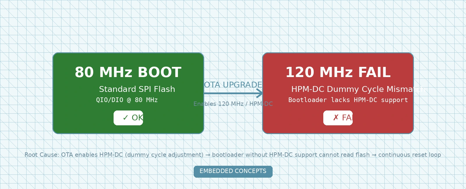
An ESP32-S3 device runs stably at an 80 MHz SPI flash clock. To maximize execution speed and SPI bus throughput, you push an Over-The-Air (OTA) firmware update configuring the flash frequency to 120 MHz. The new binary downloads, verifies, and triggers a system restart. The device boots cleanly once into the new firmware.
However, the moment a subsequent warm reset occurs — whether triggered by esp_restart(), a task watchdog reset (TWDT), or a soft reboot — the device bricks into a persistent reset loop. The UART console reports continuous invalid header: 0xffffffff errors. The second-stage bootloader never loads the application.
This failure mode is documented in Espressif Systems Bug Advisory AR2024-010 (“Software Reset Failure on ESP32-S3 After OTA Upgrade to Specific ESP-IDF Versions with Quad SPI Flash Access Frequency Increased to 120 MHz”, released October 2024). The root cause stems from a hardware-state mismatch: High Performance Mode with Dummy Cycle adjustment (HPM-DC) modifies the internal read latency registers inside the SPI NOR flash. Because 3.3V VDD power remains continuously applied across soft resets, the external flash retains these high-frequency dummy cycles. If the on-chip second-stage bootloader was compiled without HPM-DC support, its early flash read timings sample the bus out-of-phase, reading corrupted data and halting system startup.
Engineers maintaining fleets of ESP32-S3 modules encounter this specific symptom progression during field updates:
1. Factory baseline: Device ships with second-stage bootloader built on ESP-IDF v5.1.2 (no HPM-DC awareness).2. OTA update payload: Application firmware enables CONFIG_ESPTOOLPY_FLASHFREQ_120M=y.3. First reboot: Flash remains in default 80 MHz timing; legacy bootloader loads the 120 MHz app successfully.4. Application init: Application runtime configures flash registers for HPM-DC (extra dummy cycles).5. Subsequent warm reset: esp_restart() or watchdog fires; VDD rail stays hot; flash retains HPM-DC state.6. Catastrophic bootloop: Second-stage bootloader reads flash using 80 MHz dummy cycles -> Bus misalignment -> Invalid header.
The failure is insidious because post-OTA automated verification tests typically confirm that the new image boots once. The critical breakdown only surfaces on the subsequent warm reset, which often happens hours or days later in the field.
This defect presents severe operational risks for mission-critical and remote embedded deployments:
esp_ota_mark_app_valid_cancel_rollback() executes after the initial boot. Because the flash dummy cycle reconfiguration occurs during the new firmware run, the vulnerability is primed only for the next reset.invalid header: 0xffffffff) mirrors flash memory corruption, solder joint micro-fractures, or power rail brownouts. Engineering teams often waste weeks auditing PCB hardware before uncovering the software configuration conflict.External SPI NOR flash memories (e.g., Winbond W25Q series, GigaDevice GD25Q series, ISSI IS25WP series) support standard SPI, Dual SPI (DIO/DOUT), and Quad SPI (QIO/QOUT). At clock frequencies up to 80 MHz, standard access timings allow the host microcontroller to sample data reliably after default dummy cycle intervals.
When clock rates scale to 120 MHz, the period shrinks drastically:
Clock Period and Access Timing Comparison:Frequency: 80 MHzT_clk = 1 / (80 MHz) = 12.50 nsFlash Output Delay (t_v): ~6.50 ns maxTrace Propagation Delay (t_prop): ~1.00 ns (round trip)Host Input Setup Time (t_su): ~2.00 nsTotal Access Delay = t_v + t_prop + t_su = 9.50 nsTiming Margin = T_clk - 9.50 ns = 12.50 ns - 9.50 ns = +3.00 ns (Valid single-cycle latch)Frequency: 120 MHzT_clk = 1 / (120 MHz) = 8.33 nsTotal Access Delay = t_v + t_prop + t_su = 9.50 nsTiming Margin = T_clk - 9.50 ns = 8.33 ns - 9.50 ns = -1.17 ns (Violates setup budget)
Because total propagation and output valid time (9.50 ns) exceeds the 120 MHz clock period (8.33 ns), the memory controller cannot reliably latch data on the immediately adjacent clock edge. The SPI flash must operate in High Performance Mode (HPM), adjusting its internal Dummy Cycle (DC) configuration (often stored in volatile Status Register 3 or vendor configuration registers) from the default 6 dummy cycles up to 8 or 10 dummy cycles for Fast Read QIO (0xEB) and DIO (0xBB) operations.
These dummy cycles provide the internal flash sense amplifiers and output buffers the latency required to drive the data bus lines (IO0-IO3) cleanly before the host samples them:
+-----------------------------------------------------------------------------+| SPI READ BUS TIMING & DUMMY CYCLE SAMPLING MISALIGNMENT |+-----------------------------------------------------------------------------+| || FAST READ QIO (0xEB) TRANSACTION PHASES: || [ Command 0xEB ] [ 24-bit Flash Address ] [ Dummy Latency ] [ Data Out ] || || SCENARIO A: Normal 80 MHz Operation (6 Dummy Cycles Expected by Bootloader)|| SPI CLK : _|--|_|--|_|--|_|--|_|--|_|--|_|--|_|--|_|--|_|--|_|--|_ || Dummy Cyc: | 1 | 2 | 3 | 4 | 5 | 6 | || Flash Out: -----[ High-Z / Latency Wait ]----->[ Valid Data D0-D3 ] || Boot Sample: ^ Sample Edge (0xE9 OK) || || SCENARIO B: 120 MHz Flash with Legacy Bootloader After Warm Reset || (Flash chip programmed for 10 dummy cycles; Bootloader expects 6 cycles) || SPI CLK : _|--|_|--|_|--|_|--|_|--|_|--|_|--|_|--|_|--|_|--|_|--|_ || Flash DC : | 1 | 2 | 3 | 4 | 5 | 6 | 7 | 8 | 9 | 10 | || Flash Out: -----[ High-Z / Flash Internal Latency Wait ]------>[ Data ] || Boot Sample: ^ Host Samples Early || Bus State: [ Floating / 0xFFFFFFFF ] || Result : INVALID HEADER (0xFF != 0xE9)|| |+-----------------------------------------------------------------------------+
The critical vulnerability lies in the volatility profile of the SPI flash status registers:
esp_restart(), RTC watchdog, or Timer Group watchdog, the external 3.3V power regulator remains fully energized. The SPI flash never loses VDD. Consequently, the flash chip retains its modified HPM-DC status register configuration.The ESP32-S3 architecture divides the boot sequence into two distinct firmware layers:
+-----------------------------------------------------------------------+| ESP32-S3 BOOT SEQUENCE FLOW |+-----------------------------------------------------------------------+| || +-----------------------------------------------------------------+ || | 1. FIRST-STAGE BOOTLOADER (Internal Mask ROM) | || | - Executes immediately at power-on or hardware reset | || | - Reads 2nd-stage bootloader header from flash offset 0x0 | || | - Operates using conservative DOUT mode @ 80 MHz | || +-----------------------------------------------------------------+ || | || | [Loads bootloader into IRAM] || v || +-----------------------------------------------------------------+ || | 2. SECOND-STAGE BOOTLOADER (ESP-IDF bootloader.bin) | || | - Reconfigures SPI bus (QIO/DIO mode, configured clock) | || | - Parses partition table at offset 0x8000 | || | - Reads & validates active application header at 0x10000 | || +-----------------------------------------------------------------+ || | || | [Transfers execution to app] || v || +-----------------------------------------------------------------+ || | 3. APPLICATION FIRMWARE RUNTIME | || | - Calls spi_flash_hpm_enable() for 120 MHz operation | || | - Programs high-speed dummy cycles into flash Status Reg 3 | || | - Operates flash with altered internal read latency | || +-----------------------------------------------------------------+ || | || | [Warm Reset: esp_restart/Watchdog] || v || +-----------------------------------------------------------------+ || | 4. WARM RESET STATE (VDD remains applied to SPI Flash) | || | - ESP32-S3 digital logic resets | || | - SPI flash stays powered -> Retains HPM-DC dummy cycles | || +-----------------------------------------------------------------+ || | || | [ROM re-executes; loads 2nd-stage] || v || +-----------------------------------------------------------------+ || | 5. BOOTLOADER RE-ENTRY (MISMATCH FAILURE) | || | - Legacy 2nd-stage bootloader assumes DEFAULT dummy cycles | || | - Samples SPI bus out-of-phase -> Reads 0xFFFFFFFF | || | - Triggers 'invalid header' -> Infinite reboot loop | || +-----------------------------------------------------------------+ || |+-----------------------------------------------------------------------+
+-------------+---------------+----------------+----------------------+| Component | Bus Mode | HPM-DC Support | Boot Behavior |+-------------+---------------+----------------+----------------------+| 1st-stage | DOUT / DIO | N/A (Standard | Loads 2nd-stage || (Mask ROM) | @ 80 MHz | hardcoded wait)| bootloader into IRAM |+-------------+---------------+----------------+----------------------+| 2nd-stage | QIO / DIO / | NO (Built on | Reads shifted data; || (Legacy) | QOUT @ 80 MHz | old ESP-IDF) | "invalid header" |+-------------+---------------+----------------+----------------------+| Application | QIO / DIO | YES (Built for | Programs flash DC; || (New OTA) | @ 120 MHz | 120 MHz) | runs until next reset|+-------------+---------------+----------------+----------------------+
When the second-stage bootloader, built without CONFIG_BOOTLOADER_FLASH_DC_AWARE, takes control after a warm reset, it configures the internal SPI cache controller to read the partition table and application image header using standard dummy cycles (6 cycles).
However, the flash chip is waiting for 8 or 10 dummy cycles before asserting data on the bus. When the ESP32-S3 SPI controller samples the bus lines on clock cycles 6 through 9, the flash outputs are still tri-stated (high impedance with weak pull-ups). The controller samples all 1s (0xFF), missing the 0xE9 (ESP_IMAGE_HEADER_MAGIC) byte entirely. The bootloader aborts image loading with Invalid header: 0xffffffff and immediately triggers another reset.
Espressif Bug Advisory AR2024-010 defines the specific ESP-IDF release matrix where this behavior occurs:
+-----------------+------------------------+---------------+------------+| ESP-IDF Branch | Affected Version Range | Fixed Version | Commit ID |+-----------------+------------------------+---------------+------------+| release/v4.4 | v4.4.4 - v4.4.6 | v4.4.7 (EOL) | 5684098 |+-----------------+------------------------+---------------+------------+| release/v5.0 | v5.0.0 - v5.0.6 | v5.0.7 | 50fc2bf |+-----------------+------------------------+---------------+------------+| release/v5.1 | v5.1.0 - v5.1.3 | v5.1.4 | db2a037 |+-----------------+------------------------+---------------+------------+| release/v5.2+ | Not affected (Manual) | v5.2.0 | d2d75ef |+-----------------+------------------------+---------------+------------+
In affected ESP-IDF versions (such as v5.1.0 through v5.1.3), selecting CONFIG_ESPTOOLPY_FLASHFREQ_120M=y in the application configuration implicitly forced CONFIG_SPI_FLASH_HPM_DC=y during compilation. The application binary automatically linked components/spi_flash/spi_flash_hpm_enable.c and programmed the flash status registers on startup.
In the patched versions (v4.4.7, v5.0.7, v5.1.4, v5.2+):
CONFIG_BOOTLOADER_FLASH_DC_AWARE=y
CONFIG_BOOTLOADER_FLASH_DC_AWARE is active, the second-stage bootloader forces initial flash communication through DOUT mode, queries the flash state, and explicitly restores standard dummy cycle parameters before handing control over to the application image.If your device manufacturing process or OTA architecture permits bootloader reflashing, rebuild the bootloader using a patched ESP-IDF release (>= v5.1.4 or >= v5.2.0) with explicit DC awareness:
# In the project workspace, open menuconfigidf.py menuconfig# Navigate to:# Security features / Bootloader config ---># [*] Allow app adjust Dummy Cycle bits in SPI Flash for higher frequency (CONFIG_BOOTLOADER_FLASH_DC_AWARE)# Build the second-stage bootloader binary independentlyidf.py bootloader# Flash the updated bootloader to flash offset 0x0 (ESP32-S3)esptool.py --chip esp32s3 --port /dev/ttyUSB0 --baud 460800 \write_flash 0x0 build/bootloader/bootloader.bin
When running, the updated bootloader logs its DC awareness state:
I (125) boot: ESP-IDF v5.1.4I (128) boot: Flash DC aware: yesI (133) boot: Flash freq: 120 MHzI (138) boot: Flash mode: QIO
If thousands of legacy devices are already in customer hands and your OTA infrastructure cannot safely update the bootloader partition at offset 0x0, do not configure 120 MHz in application OTA updates.
Cap the flash access frequency at 80 MHz in sdkconfig:
# Disable 120 MHz flash frequencyCONFIG_ESPTOOLPY_FLASHFREQ_120M=n# Revert to stable 80 MHz flash frequencyCONFIG_ESPTOOLPY_FLASHFREQ_80M=yCONFIG_ESPTOOLPY_FLASHFREQ="80m"
Operating at 80 MHz eliminates the requirement for HPM-DC. The application will never touch the flash chip’s Dummy Cycle status bits, ensuring that legacy bootloaders remain 100% compatible across all reset scenarios.
If a device is currently cycling in the invalid header loop:
To prevent remote devices from applying an OTA payload that will brick them upon the next reset, embed an explicit bootloader compatibility check into the application’s OTA update worker.
The application inspects the active bootloader binary metadata using esp_ota_get_bootloader_description():
// ota_compatibility_guard.c#include <string.h>#include "esp_log.h"#include "esp_err.h"#include "esp_ota_ops.h"#include "esp_bootloader_desc.h"static const char *TAG = "OTA_GUARD";/*** @brief Checks if the running bootloader supports HPM-DC (Dummy Cycle Awareness).** @return true if the bootloader is patched and safe for 120 MHz flash operation.* @return false if the bootloader is legacy and vulnerable to AR2024-010.*/bool is_bootloader_safe_for_120mhz(void) {esp_bootloader_desc_t bl_desc;// Passing NULL targets the primary second-stage bootloader at offset 0x0esp_err_t err = esp_ota_get_bootloader_description(NULL, &bl_desc);if (err != ESP_OK) {ESP_LOGE(TAG, "Failed to read bootloader descriptor: %s", esp_err_to_name(err));return false;}ESP_LOGI(TAG, "Bootloader App Version: %s", bl_desc.version);ESP_LOGI(TAG, "Bootloader Compiled IDF: %s", bl_desc.idf_ver);// Verify whether the bootloader was compiled with patched IDF releases// Patched versions: v4.4.7+, v5.0.7+, v5.1.4+, v5.2.0+if (strstr(bl_desc.idf_ver, "v5.1.4") != NULL ||strstr(bl_desc.idf_ver, "v5.2") != NULL ||strstr(bl_desc.idf_ver, "v5.3") != NULL ||strstr(bl_desc.idf_ver, "v5.4") != NULL ||strstr(bl_desc.idf_ver, "v5.0.7") != NULL ||strstr(bl_desc.idf_ver, "v4.4.7") != NULL) {ESP_LOGI(TAG, "Bootloader supports HPM-DC awareness. 120 MHz safe.");return true;}ESP_LOGW(TAG, "Legacy bootloader detected (%s). 120 MHz OTA prohibited!", bl_desc.idf_ver);return false;}/*** @brief Pre-OTA validation handler.*/esp_err_t validate_ota_target_payload(bool incoming_payload_uses_120mhz) {if (incoming_payload_uses_120mhz) {if (!is_bootloader_safe_for_120mhz()) {ESP_LOGE(TAG, "Aborting OTA: Target image requires 120 MHz HPM-DC, ""but active bootloader is not DC-aware.");return ESP_ERR_NOT_SUPPORTED;}}return ESP_OK;}
Not all flash silicon models behave identically in High Performance Mode. Before enabling high-speed modes, verify that the mounted flash chip matches supported vendor specifications:
// spi_flash_hardware_check.c#include "esp_log.h"#include "esp_err.h"#include "esp_flash.h"static const char *TAG = "FLASH_PROBE";/*** @brief Reads JEDEC ID and confirms HPM-DC hardware compatibility.*/bool verify_flash_hardware_compatibility(void) {uint32_t raw_id = 0;// Read JEDEC ID from the default primary SPI flashesp_err_t err = esp_flash_read_id(NULL, &raw_id);if (err != ESP_OK) {ESP_LOGE(TAG, "Failed to read SPI flash JEDEC ID: %s", esp_err_to_name(err));return false;}// ESP-IDF packs JEDEC ID as:// Bits [23:16]: Manufacturer ID// Bits [15:0] : Memory Type & Capacity (Chip ID)uint8_t mfg_id = (uint8_t)((raw_id >> 16) & 0xFF);uint16_t chip_id = (uint16_t)(raw_id & 0xFFFF);ESP_LOGI(TAG, "SPI Flash JEDEC ID: 0x%06lX (Mfg: 0x%02X, Chip: 0x%04X)",(unsigned long)raw_id, mfg_id, chip_id);switch (mfg_id) {case 0xEF: // Winbond Electronics// W25Q128JV (0x4018), W25Q256JV (0x4019), W25Q-DTR (0x6018+)if ((chip_id & 0xFF) >= 0x18) {ESP_LOGI(TAG, "Identified Winbond >=128Mbit flash with HPM support.");return true;}break;case 0xC8: // GigaDevice// GD25Q128 (0x4018), GD25Q256 (0x4019)if ((chip_id & 0xFF) >= 0x18) {ESP_LOGI(TAG, "Identified GigaDevice >=128Mbit flash with HPM support.");return true;}break;case 0x9D: // ISSI (Integrated Silicon Solution Inc.)// IS25WP128 (0x7018), IS25WP256 (0x7019)if ((chip_id & 0xFF) >= 0x18) {ESP_LOGI(TAG, "Identified ISSI >=128Mbit flash with HPM support.");return true;}break;case 0xC2: // Macronix// MX25U12835 (0x2538)if (chip_id >= 0x2538) {ESP_LOGI(TAG, "Identified Macronix high-speed flash with HPM support.");return true;}break;default:ESP_LOGW(TAG, "Unknown flash manufacturer 0x%02X. Proceed with caution at 120MHz.", mfg_id);return false;}ESP_LOGW(TAG, "Flash capacity too low (<128Mbit) or unsupported chip ID 0x%04X.", chip_id);return false;}
+--------------+------------------+----------------+----------------+| Manufacturer | Flash Series | JEDEC Mfg ID | Chip ID Range |+--------------+------------------+----------------+----------------+| Winbond | W25Q-JV / JW | 0xEF | 0x4018 - 0x4019|| (0xEF) | W25Q-DW (DTR) | 0xEF | 0x6018 - 0x6019|+--------------+------------------+----------------+----------------+| GigaDevice | GD25Q series | 0xC8 | 0x4018 - 0x4019|| (0xC8) | GD25LT series | 0xC8 | 0x6018 - 0x6019|+--------------+------------------+----------------+----------------+| ISSI | IS25WP series | 0x9D | 0x7018 - 0x7019|| (0x9D) | IS25LP series | 0x9D | 0x6018 - 0x6019|+--------------+------------------+----------------+----------------+| Macronix | MX25U series | 0xC2 | 0x2538 - 0x2539|| (0xC2) | MX25L series | 0xC2 | 0x2018 - 0x2019|+--------------+------------------+----------------+----------------+
Before generating release binaries, verify your build system settings:
# 1. Verify ESP-IDF checkout version tagcd $IDF_PATH && git describe --tags# Must report v5.1.4, v5.0.7, v4.4.7, or >= v5.2.0# 2. Inspect bootloader build configurationgrep "CONFIG_BOOTLOADER_FLASH_DC_AWARE" build/bootloader/sdkconfig# Expected output: CONFIG_BOOTLOADER_FLASH_DC_AWARE=y# 3. Inspect application flash frequency settinggrep "CONFIG_ESPTOOLPY_FLASHFREQ" sdkconfig# Expected output: CONFIG_ESPTOOLPY_FLASHFREQ_120M=y (if bootloader is DC-aware)# OR: CONFIG_ESPTOOLPY_FLASHFREQ_80M=y (if legacy bootloader fleet)
Monitor the UART output during cold boot and subsequent warm resets:
ESP-ROM:esp32s3-20210327Build:Mar 27 2021rst:0x1 (POWERON),boot:0x2b (SPI_FAST_FLASH_BOOT)SPIWP:0xeemode:DIO, clock div:1load:0x3fce3808,len:0x170cload:0x403c9700,len:0xa10load:0x403cc700,len:0x2f64entry 0x403c98dcI (125) boot: ESP-IDF v5.1.4I (128) boot: Flash DC aware: yesI (133) boot: Flash freq: 120 MHzI (138) boot: Flash mode: QIOI (143) boot: Loading app from 0x10000...I (150) boot: Application validation successful. Starting main runtime.
ESP-ROM:esp32s3-20210327Build:Mar 27 2021rst:0x3 (RTC_SW_SYS_RST),boot:0x2b (SPI_FAST_FLASH_BOOT)SPIWP:0xeemode:DIO, clock div:1load:0x3fce3808,len:0x170cload:0x403c9700,len:0xa10load:0x403cc700,len:0x2f64entry 0x403c98dcI (123) boot: ESP-IDF v5.1.2I (125) boot: Flash DC aware: noE (130) boot: Invalid header: 0xffffffffE (132) boot: Bootloader checksum failedrst:0x7 (TG0WDT_SYS_RST),boot:0x2b (SPI_FAST_FLASH_BOOT)... (repeats indefinitely)
Connecting a high-bandwidth logic analyzer (>= 500 MSa/s) or oscilloscope to SPI_CLK, SPI_CS, and SPI_D0-SPI_D3 reveals the physical bus breakdown during the warm reset:
+-----------+-------------------------------+----------------------+| Boot Phase| Expected Normal Signal State | Mismatch Failure Mode|+-----------+-------------------------------+----------------------+| 1st-stage | ROM issues DOUT @ 80 MHz; | Normal execution; || (ROM) | standard latency cycles | loads 2nd-stage |+-----------+-------------------------------+----------------------+| 2nd-stage | Controller reads partition / | Host samples after 6 || header | app header expecting 6 cycles;| cycles; flash drives || read | flash delivers on cycle 6 | on cycle 8 -> 0xFF |+-----------+-------------------------------+----------------------+| App load | Flash DC aware bootloader | App validation aborts|| | resets DC or matches timing; | due to bad header; || | valid magic byte 0xE9 read | reset loop triggered |+-----------+-------------------------------+----------------------+
The ESP32-S3 post-OTA bootloop at 120 MHz SPI flash frequency is a system architecture compatibility defect, not a catastrophic silicon breakdown. When firmware enables High Performance Mode with Dummy Cycle adjustment (HPM-DC), the external SPI flash stores the extra latency cycles in its volatile configuration registers. Because 3.3V power is maintained across soft restarts, the flash retains these settings while the legacy second-stage bootloader expects standard 80 MHz timing.
Core Resolution Matrix:
CONFIG_BOOTLOADER_FLASH_DC_AWARE=y.CONFIG_ESPTOOLPY_FLASHFREQ_80M=y.Treat the second-stage bootloader and application as an atomic, co-dependent pair. Any OTA upgrade that alters peripheral bus timing, wait states, or interface clock frequencies must verify bootloader compatibility prior to executing the update transaction.
+-------------------------------------------------------------------------+| HPM-DC OTA BOOTLOOP PROGRESSION & FIX |+-------------------------------------------------------------------------+| || [ FACTORY BASELINE ] || Bootloader v5.1.2 (Legacy, no DC_AWARE) + Application @ 80 MHz || | || | OTA Update (App bumped to 120 MHz, FLASHFREQ_120M) || v || [ FIRST SYSTEM REBOOT ] || Flash still has power-on default dummy cycles (6 cycles) || Legacy bootloader loads new 120 MHz application successfully || | || | Application startup executes spi_flash_hpm_enable() || v || [ RUNTIME HPM-DC ACTIVATION ] || Application writes Flash Status Register 3 (Dummy Cycles: 6 -> 8 or 10)|| High-speed QIO/DIO reads function properly while application runs || | || | System triggers WARM RESET (esp_restart, TWDT, or pin reset) || v || [ WARM RESET OCCURS ] || MCU resets; 3.3V VDD to SPI flash remains continuously powered || Flash chip retains modified dummy cycle setting (8 or 10 cycles) || | || | ROM loads legacy second-stage bootloader || v || [ SECOND-STAGE BOOTLOADER READ MISMATCH ] || Legacy bootloader configures host SPI controller for DEFAULT 6 cycles || Flash memory holds data until cycle 8/10 -> Host samples floating bus || | || | Bus reads 0xFFFFFFFF instead of magic byte 0xE9 || v || +-------------------------------------------------------------------+ || | BOOT FAILURE LOOP: 'Invalid header: 0xffffffff' -> Constant Reset | || +-------------------------------------------------------------------+ || | || +-------------------------------+ || | | || | [Emergency Field Recovery] | [Permanent Prevention] || v v || +-----------------------------+ +-----------------------------------+ || | COLD POWER CYCLE | | UPDATE BOOTLOADER | || | Drop VDD to 0V completely | | Build with ESP-IDF >= v5.1.4 | || | Flash volatile registers POR| | Set CONFIG_BOOTLOADER_FLASH_ | || | Reverts to 6 dummy cycles | | DC_AWARE=y | || | Device boots cleanly once | | Restores DC before reading app | || +-----------------------------+ +-----------------------------------+ || |+-------------------------------------------------------------------------+
Quick Links
Legal Stuff